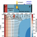
 “Depletion region surface effects in electron beam induced current measurements”, P. M. Haney, H. P. Yoon, B. Gaury, and N. B. Zhitenev , J. of Appl. Phys. 120, 105095702, 2016.
1. Center for Nanoscale Science and Technology, National Institute of Standards and Technology, Gaithersburg, Maryland 20899, USA; 2. Department of Electrical and Computer Engineering, University of Utah, Salt Lake City, Utah 84112, USA; 3. Maryland NanoCenter, University of Maryland, College Park, Maryland 20742.
ABSTRACT. Electron beam induced current (EBIC) is a powerful characterization technique which offers the high spatial resolution needed to study polycrystalline solar cells. Current models of EBIC assume that excitations in the p-n junction depletion region result in perfect charge collection efficiency. However, we find that in CdTe and Si samples prepared by focused ion beam (FIB) milling, there is a reduced and nonuniform EBIC lineshape for excitations in the depletion region. Motivated by this, we present a model of the EBIC response for excitations in the depletion region which includes the effects of surface recombination from both charge-neutral and charged surfaces. For neutral surfaces, we present a simple analytical formula which describes the numerical data well, while the charged surface response depends qualitatively on the location of the surface Fermi level relative to the bulk Fermi level. We find that the experimental data on FIB-prepared Si solar cells are most consistent with a charged surface and discuss the implications for EBIC experiments on polycrystalline materials.

