[ECE 6960-006] Advanced Electron Microscopy for Semiconductor Devices
Lecture: Wednesday / Thursday 2:00 pm ~ 2:50 pm
Prelab Friday 2:00 pm ~ 2: 50 pm
Lab: Tuesday (2-hour labs at the Nanofab; details: TBA)
Course Objectives
The goal of this course is to introduce the students to both the theory and practical use of modern scanning electron microscopy (SEM) for micro/nano materials and devices. We will start from the principle of electron microscopy, proceed to the description of conventional and advanced modern technique, and evaluate advantages and disadvantages of each method.
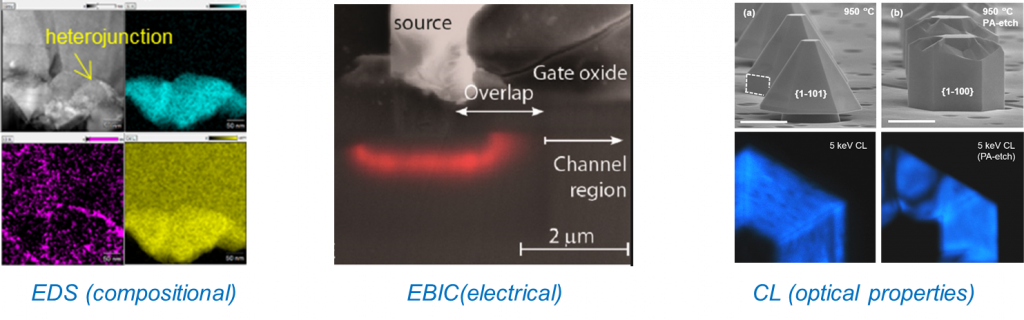
In particular, we will focus on metrologies for semiconductors devices, such as energy dispersive X-ray spectroscopy (EDX), electron beam induced current (EBIC), and cathodoluminescence (CL), to study active defects, junction interfaces, and excess carrier dynamics of the devices. The lab sessions will be held in the state-of-the-art laboratories of the Utah’s Nanofab. We will also use software to perform simulations and data analysis. Students will understand what studies can be addressed with each technique and what is the level of details that can be expected. This course is also designed to provide students from various field a practical introduction to nanoscale electrical and optical measurements of emerging semiconductor materials and devices.