

“Nanoscale imaging and spectroscopy of band gap and defects in polycrystalline photovoltaic devices”, Y. Yoon1, 2, J. Chae1, 2, A. M. Katzenmeyer1, H. P. Yoon1,2,3, J. Schumacher1, S. An1, A. Centronea1, and N. Zhitenev1, Nanoscale 9, 7771, 2017.
1. Center for Nanoscale Science and Technology, National Institute of Standards and Technology, Gaithersburg, Maryland 20899, USA;
2. Maryland Nanocenter, College Park, Maryland 02421, USA;
3. Dept. of Electrical & Computer Engineering, University of Utah, Salt Lake City, Utah 84112, USA.
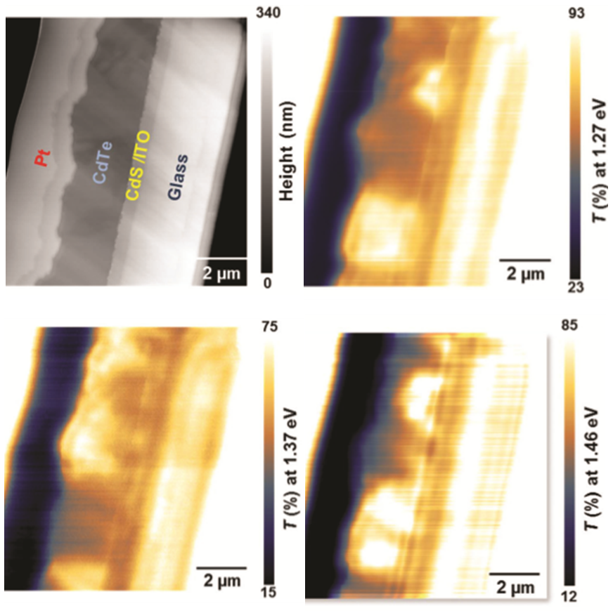
ABSTRACT. Improving the power conversion efficiency of photovoltaic (PV) devices is challenging because the generation, separation and collection of electron–hole pairs are strongly dependent on details of the nanoscale chemical composition and defects which are often poorly known. In this work, two novel scanning probe nano-spectroscopy techniques, direct-transmission near-field scanning optical microscopy (dt-NSOM) and photothermal induced resonance (PTIR), are implemented to probe the distribution of defects and the bandgap variation in thin lamellae extracted from polycrystalline CdTe PV devices. dt-NSOM provides high-contrast spatially-resolved maps of light transmitted through the sample at selected wavelengths. PTIR provides absorption maps and spectra over a broad spectral range, from visible to mid-infrared. Results show variation of the bandgap through the CdTe thickness and from grain to grain that is spatially uncorrelated with the distributions of shallow and deep defects.