

 “Observation and Implications of Composition Inhomogeneity Along Grain Boundaries in Thin Film Polycrystalline CdTe Photovoltaic Devices“, S. Misra1, J. A. Aguiar2, Y. Sun3, B. V. Devener2, V. Palekis4, C. S. Ferekides4, H. P. Yoon1, P. Bermel3, M. A. Scarpulla1, Advanced Materials Interfaces 1900152, 2019.
1. Electrical and Computer Engineering, University of Utah, Salt Lake City, UT 84102, USA
2. Nuclear Materials Department, Idaho National Laboratory, Idaho Falls, ID 83415, USA
3. Electrical and Computer Engineering, Purdue University, West Lafayette, IN 47906, USA
4. Electrical Engineering, University of South Florida, Tampa, FL 33620, USA
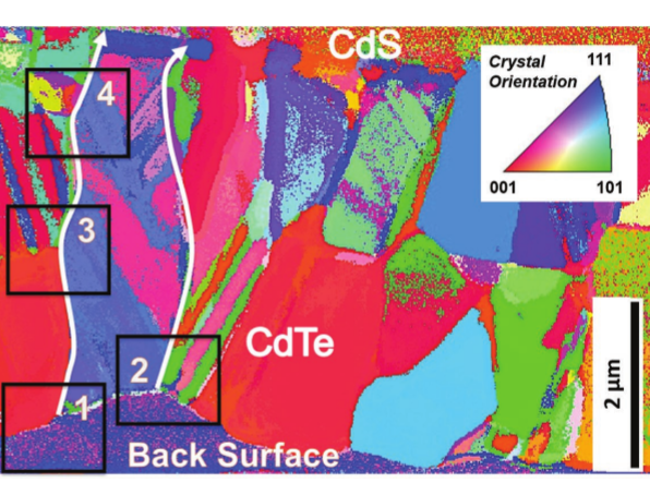
Leading photovoltaic technologies such as multicrystalline Si, CdTe, Cu(In,Ga)Se2, and lead halide perovskites are polycrystalline, yet achieve relatively high performance. At the moment polycrystalline photovoltaic technologies stand at a juncture where further advances in device performance and reliability necessitate additional characterization and modeling to include nanoscale property variations. Properties and implications of grain boundaries are previously studied, yet chemistry variations along individual grain boundaries and its implications are not yet fully explored. Here, the effects of bromine etching of CdTe absorber layers on the nanoscale chemistry are reported. Bromine etching is commonly used for improving CdTe back contacts, yet it removes both cadmium and chlorine along grain boundaries to depths closer to 1 µm. 2D device simulations reveal these composition modifications limit photovoltaic performance. Since grain boundaries and their intersections with surfaces and interfaces are universal to thin film photovoltaics, these findings call for similar studies in each of the photovoltaic technologies to further enable advances.