
The Army Research Lab visited the University of Utah. Dr. Yoon and David attended the technical sessions and provided a lab tour to the program managers. We also discussed the recent development on integrated solar cells.
Author: HPY
2018 11 Video Tutorial (e-beam simulator; PART 2)
Second video tutorial for Monte Carlo Simulation of Electron Trajectory in Solid, taught by Dean Collett.
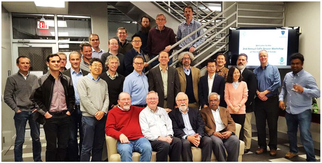
2018 10 CdTe PV Workshop in Toledo, OH
Dr. Yoon attended the 2nd PV workshop and gave two talks. The focus of the workshop is to initiate a closer research community and identification of opportunities for collaborative research, specifically in CdTe.
2018 09 Popular SEM demo by David (Global Class Program)
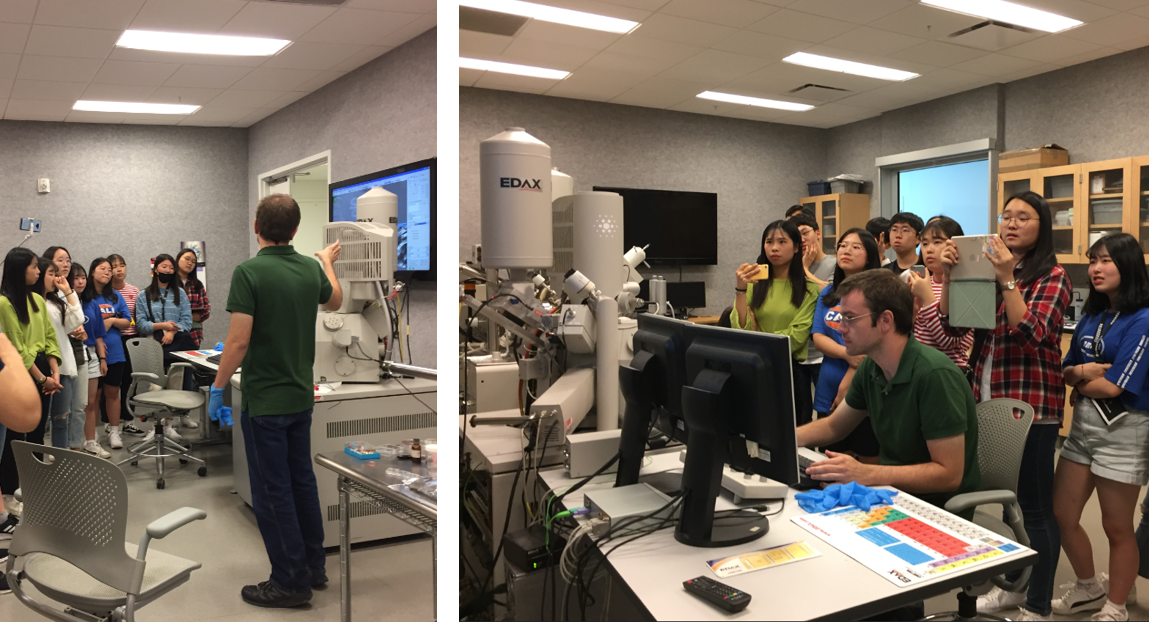 We welcome Neugju high-school students visiting the University of Utah (Global Engagement Program). David Magginetti (PhD student in Yoon’s group) gave a brief introduction and a demo on scanning electron microscope (SEM). We looked at a coin (10 won) to find a secrete feature in the middle of the pagoda (DaBoTap). Ask students from Neungju High School (South Korea) what they found!
2018 09 Invited Talks at the Regional Workshops
Dr. Yoon attended the regional workshops and gave a talk on an integrated PV system.
- RF and Wireless Day (September 12, Utah State University)
- Advancing the Development Cycle Through Intelligent Materials Design, Informatics, and Characterization (September 6, Colorado School of Mines)
2018 08 Microscopy and Microanalysis (M&M) Conference
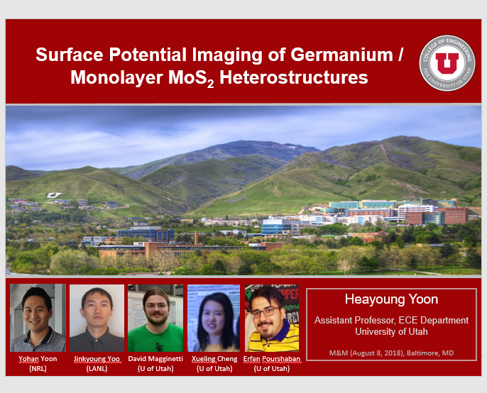
A collaborative work with NIST (National Institute of Standards and Technology) and LANL (Los Alamos National Laboratory) was presented at the M&M conference (Baltimore, MD).
https://doi.org/10.1017/S1431927618008498
2018 07 Dr. Yoon gives a talk at technical workshops.
Dr. Yoon discussed the recent research progress made by Erfan and David, and shared the new project direction of her group.
- U.S. Air Force Science and Technology 2030 (July 10, Salt Lake City, UT)
- Materials in Space Workshop by CASIS (Center for the Advancement of Science in Space)/NSF (July 21, San Francisco, CA)
2018 07 Video Tutorial (e-beam simulator; PART 1)
A short video tutorial for Monte Carlo Simulation of Electron Trajectory in Solid, taught by Dean Collett. Dean, thank you for sharing the nice video with us!
2018 07 Electronic Materials Conference
Yoon’s group presented two research projects at the 60th EMC conference (June 27 ~ June 29, 2018; University of California, Santa Barbara, CA)
♦ Large-area MoTe2 Film Growth Using High-Vacuum Ampoule Process (David Magginetti, Xueling Cheng, Prashanth Gopalan, BerardiSensale-Rodriguez, and Heayoung Yoon)
♦ Local Photovoltage / NSOM Imaging of ZnTe/CdTe Back Contact (Yohan Yoon, David Magginetti, Erfan Pourshaban, Vasilios Palekis, Chih An Hsu, Mike Scarpulla, Chris Ferekides, and Heayoung Yoon)
2018 06 Yoon wins Research Incentive Seed Grant.
![]() We are excited about the new project related with a novel nanostructured PV/cooling system. We appreciate the support from the VPR office at the U.
We are excited about the new project related with a novel nanostructured PV/cooling system. We appreciate the support from the VPR office at the U.