
Yang and Dean received their BS degree today. Lots of congratulations! Yang will continue her MS program at the U. Dean is seeking for a job near Salt Lake City. If you are looking for one of our best graduates (Dean’s list), here is one of them (Dean Collett: deanacollett@gmail.com).
Author: HPY
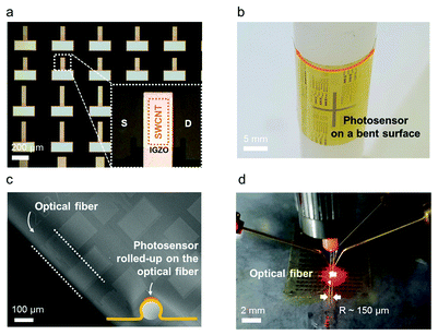
2018 04 “I support my friends.” (Technical Open-House)
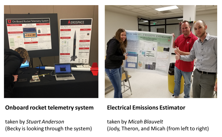
2017 Nanoscale
 “Wide-spectral/dynamic-range skin-compatible phototransistors enabled by floated heterojunction structures with surface functionalized SWCNTs and amorphous oxide semiconductors“, I. Hwang1, J. Kim1, M. Lee2, M. Lee1, H. Kim1, H. Kwon1, D. Hwang3, M. Kim4, H. Yoon5, Y. Kim2, and S. Park1, Nanoscale 9, 16711, 2017.
1. School of Electrical and Electronics Engineering, Chung-Ang University, Seoul 06974, Korea
2. School of Advanced Materials Science and Engineering and SKKU Advanced Institute of Nanotechnology (SAINT), Sungkyunkwan University, Suwon, Korea
3. Center for Opto-Electronic Materials and Devices, Post-Silicon Semiconductor Institute, Korea Institute of Science and Technology (KIST), Seoul, Korea
4. Department of Chemistry, Chung-Ang University, Seoul, Korea
5. Department of Electrical and Computer Engineering, University of Utah, Salt Lake City, USA
Read more
2017 10 Welcome Yohan!
We welcome a new group member, Dr. Yohan Yoon. Yohan will continue working at CNST/NIST on the project of nanoscale local characterizations of PV devices and emerging semiconductor materials.
2017 09 Dr. Yoon teaches a new course (eMicroscopy)
[ECE 6960-006] Advanced Electron Microscopy for Semiconductor Devices
Lecture: Wednesday / Thursday 2:00 pm ~ 2:50 pm
Prelab Friday 2:00 pm ~ 2: 50 pm
Lab: Tuesday (2-hour labs at the Nanofab; details: TBA)
Course Objectives
The goal of this course is to introduce the students to both the theory and practical use of modern scanning electron microscopy (SEM) for micro/nano materials and devices. We will start from the principle of electron microscopy, proceed to the description of conventional and advanced modern technique, and evaluate advantages and disadvantages of each method.
2017 08 * Andrew presents at the OUR Summer Symposium
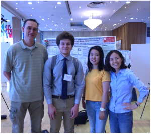 Andrew (REU student from Clarion University) gave his final presentation at the Summer Symposium organized by the Office of Undergraduate Research (OUR) at the University of Utah. It was a delightful experience having Andy in the group over the summer. Good work, Andy.
(left to right: Dean Collett, Andrew Baker, Xueling Cheng, and Yoon)
2017 07 * Outreach Program (Global Engagement)
David, Dean, and Dr. Yoon gave a lecture and a lab tour to 25 high-school students from Neungjoo High School (South Korea). We enjoyed the time with the students, who wanted to know about solar cells, nanomaterials and their characterizations. This Summer Global Class Program is part of global outreach program at the University of Utah (Office for Global Engagement).
2017 07 * Dean gives a presentation at the International Conference (EMC).
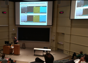 Undergraduate student, Dean Collett, gave an oral presentation at the Electronic Materials Conference (Notre Dame, IN). Good work, Dean!
2017 07 * New Grant from NSF
 Yoon’s research group receives a three-year grant from NSF in collaboration with Prof. Mike Scarpulla (ECE, University of Utah) and Prof. Christos Ferekides (EE, University of South Florida). We are excited about the new project on CdTe solar cells.
2017 07 Electronic Materials Conference
Dean’s EMC conference paper is accepted for a platform presentation at the 59th EMC Conference (June 28-30, 2017; University of Notre Dame, South Bend, ID).
2017 07 * Dean gives a presentation at the International Conference (EMC).
Heterojunction Electronic Properties and Compositional Differences of CdCl2 Post-Treated CdTe Solar Cell (Dean Collett 1, Jeffery A. Aguiar 2,3, Brian v. Devener 4, Yohan Yoon 5,6, Paul Haney 6, Nikolai Zhitenev 6, Michael Scarpulla 1,3, Prakash Koirala 7, Robert W. Collins 7 and Heayoung Yoon 1).
1. Electrical and Computer Engineering, University of Utah, Salt Lake City, Utah.
2. Fuel Design and Development Department, Idaho National Laboratory, Idaho Falls, Idaho.
3. Department of Materials Science and Engineering, University of Utah, Salt Lake City, Utah.
4. Utah Nanofab, University of Utah, Salt Lake City, Utah.
5. Maryland NanoCenter, University of Maryland, College Park, Maryland.
6. Center for Nanoscale Science and Technology, National Institute of Standards and Technology, Gaithersburg, Maryland.
7. Department of Physics and Astronomy, Center for Photovoltaics Innovation and Commercialization, University of Toledo, Toledo, Ohio