2011 Nanotechnology

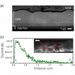
NT_SiNWSingle nanowire radial junction solar cells fabricated using Al catalyzed Si nanowires”, Y. Ke, X. Wang, C. E. Kendrick, Y. A. Yu, S. M. Eichfeld, H. P. Yoon, J. M. Redwing, T. S. Mayer, and Y. M. Habib, Nanotechnology 22, 445401, 2011.

1. Department of Materials Science and Engineering, Materials Research Institute, The Pennsylvania State University, University Park, PA 16802, USA
2. Department of Electrical Engineering, Materials Research Institute, The Pennsylvania State University, University Park, PA 16802, USA
3. Illuminex Corp., Lancaster, PA 17601, USA

ABSTRACT. Single nanowire radial junction solar cell devices were fabricated using Si nanowires synthesized by Al-catalyzed vapor–liquid–solid growth of the p+ core (Al auto-doping) and thin film deposition of the n+-shell at temperatures below 650 ◦C. Short circuit current densities of ∼11.7 mA /cm2 were measured under 1-sun AM1.5G illumination, showing enhanced optical absorption. The power conversion efficiencies were limited to <1% by the low open circuit voltage and fill factor of the devices, which was attributed to junction shunt leakage promoted by the high p+ /n+ doping. This demonstration of a radial junction device represents an important advance in the use of Al-catalyzed Si nanowire growth for low cost photovoltaics.

LINK

2010 Applied Physics Letters (NW)

apl_nwPVRadial junction silicon wire array solar cells fabricated by gold-catalyzed vapor-liquid-solid growth“, C. E. Kendrick, H. P. Yoon, Y. A. Yuwen, G. D. Barber, H. Shen, T. E. Mallouk, E. C. Dickey, T. S. Mayer, and J. M. Redwing, Applied Physics Letters 97, 143108, 2010.

1. Department of Materials Science and Engineering, The Pennsylvania State University, University Park, Pennsylvania 16802, USA
2. Department of Electrical Engineering, The Pennsylvania State University, University Park, Pennsylvania 16802, USA
3. Department of Chemistry, The Pennsylvania State University, University Park, Pennsylvania 16802, USA

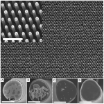
ABSTRACT. The fabrication of radial junction silicon Si solar cells using Si wire arrays grown by Au-catalyzed vapor-liquid-solid growth on patterned Si substrates was demonstrated. An important step in the fabrication process is the repeated thermal oxidation and oxide etching of the Si wire arrays. The oxidation cleaning process removes residual catalyst material from the wire tips and exposes additional Au embedded in the material. Using this cleaning process and junction formation through POCl3 thermal diffusion, rectifying p-n junctions were obtained that exhibited an efficiency of 2.3% and open circuit voltages up to 0.5 V under Air Mass 1.5G illumination.

LINK

2010 Applied Physics Letters (Pillars)

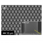
apl_pillar arrayEnhanced conversion efficiencies for pillar array solar cells fabricated from crystalline silicon with short minority carrier diffusion lengths”, H. P. Yoon, Y. A. Yuwen, C. E. Kendrick, G. D. Barber, N. J. Podraza, J. M. Redwing, T. E. Mallouk, C. R. Wronski, and T. S. Mayer, Applied Physics Letters 96, 213503, 2010.

1. Department of Electrical Engineering, The Pennsylvania State University, University Park, Pennsylvania 16802, USA
2. Department of Materials Science and Engineering, The Pennsylvania State University, University Park, Pennsylvania 16802, USA
3. Department of Chemistry, The Pennsylvania State University, University Park, Pennsylvania 16802, USA

ABSTRACT. Radial n+/p+ junction solar cells composed of densely packed pillar arrays, 25 μm-tall and 7.5 μm in diameter, fabricated from p-type silicon substrates with extremely short minority carrier diffusion lengths are investigated and compared to planar cells. To understand the two times higher AM 1.5 efficiencies of the pillar array cells, dark and light I-V characteristics as well as spectral responses are presented for the two structures. The higher pillar array cell efficiencies are due to the larger short-circuit currents from the larger photon absorption thickness and the shorter carrier collection length, with a significant additional contribution from multiple reflections in the structure.

LINK

2010 Nano Letters

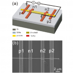
crossed-nwCrossed-nanowire molecular junctions: A new multi-spectroscopy platform for molecular conduction-structure correlations”, H. P. Yoon, M. M. Maitani, O. M. Cabarcos, L. Cai, T. S. Mayer, and D. L. Allara, Nano Letters 10 (8), 2897-2902, 2010.

1. Department of Electrical Engineering, 2. Department of Materials Science and Engineering, and 3.Department of Chemistry, The Pennsylvania State University, University Park, Pennsylvania 16802

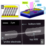
ABSTRACT. We report a crossed-nanowire molecular junction array platform that enables direct measurement of current-voltage-temperature characteristics simultaneously with inelastic electron tunneling and Raman vibrational spectra on the same junction. Measurements on dithiol-terminated oligo(phenylene-ethynylene) junctions show both spectroscopies interrogate the gap-confined molecules to reveal distinct molecular features. This versatile platform allows investigation of advanced phenomena such as molecular switching and cooperative effects with the flexible ability to scale both the junction geometries and array sizes.

LINK

2005 Nano Letters

inwire_OMAnReversible bistable switching in nanoscale thiol-substituted oligoaniline molecular junctions”, L. Cai, M. A. Cabassi, H. Yoon, O. M. Cabarcos, C. L. McGuiness, A. K. Flatt, D. L. Allara, J. M. Tour, and T. S. Mayer, Nano Letters 5 (12), 2365-2372, 2005.

1. Department of Electrical Engineering and Department of Chemistry and Materials Research Institute, The Pennsylvania State University, University Park, Pennsylvania 16802
2. Department of Chemistry and Center for Nanoscale Science and Technology, Rice University, Houston, Texas 77005

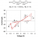
ABSTRACT. Single molecular monolayers of oligoaniline dimers were integrated into sub-40-nm-diameter metal nanowires to form in-wire molecular junctions. These junctions exhibited reproducible room temperature bistable switching with zero-bias high- to low-current state conductance ratios of up to 50, switching threshold voltages of approximately ±1.5 V, and no measurable decay in the high-state current over 22 h. Such switching was not observed in similarly fabricated saturated dodecane (C12) or conjugated oligo(phenylene ethynylene) (OPE) molecular junctions. The low- and high-state current versus voltage was independent of temperature (10-300 K), suggesting that the dominant transport mechanism in these junctions is coherent tunneling. Inelastic electron tunneling spectra collected at 10 K show a change in the vibrational modes of the oligoaniline dimers when the junctions are switched from the low- to the high-current state. The results of these measurements suggest that the switching behavior is an inherent molecular feature that can be attributed to the oligoaniline dimer molecules that form the junction.

LINK