2011 Nanotechnology

NT_SiNWSingle nanowire radial junction solar cells fabricated using Al catalyzed Si nanowires”, Y. Ke, X. Wang, C. E. Kendrick, Y. A. Yu, S. M. Eichfeld, H. P. Yoon, J. M. Redwing, T. S. Mayer, and Y. M. Habib, Nanotechnology 22, 445401, 2011.

1. Department of Materials Science and Engineering, Materials Research Institute, The Pennsylvania State University, University Park, PA 16802, USA
2. Department of Electrical Engineering, Materials Research Institute, The Pennsylvania State University, University Park, PA 16802, USA
3. Illuminex Corp., Lancaster, PA 17601, USA

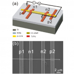
ABSTRACT. Single nanowire radial junction solar cell devices were fabricated using Si nanowires synthesized by Al-catalyzed vapor–liquid–solid growth of the p+ core (Al auto-doping) and thin film deposition of the n+-shell at temperatures below 650 ◦C. Short circuit current densities of ∼11.7 mA /cm2 were measured under 1-sun AM1.5G illumination, showing enhanced optical absorption. The power conversion efficiencies were limited to <1% by the low open circuit voltage and fill factor of the devices, which was attributed to junction shunt leakage promoted by the high p+ /n+ doping. This demonstration of a radial junction device represents an important advance in the use of Al-catalyzed Si nanowire growth for low cost photovoltaics.

LINK

2010 Applied Physics Letters (NW)

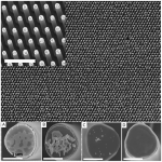
apl_nwPVRadial junction silicon wire array solar cells fabricated by gold-catalyzed vapor-liquid-solid growth“, C. E. Kendrick, H. P. Yoon, Y. A. Yuwen, G. D. Barber, H. Shen, T. E. Mallouk, E. C. Dickey, T. S. Mayer, and J. M. Redwing, Applied Physics Letters 97, 143108, 2010.

1. Department of Materials Science and Engineering, The Pennsylvania State University, University Park, Pennsylvania 16802, USA
2. Department of Electrical Engineering, The Pennsylvania State University, University Park, Pennsylvania 16802, USA
3. Department of Chemistry, The Pennsylvania State University, University Park, Pennsylvania 16802, USA

ABSTRACT. The fabrication of radial junction silicon Si solar cells using Si wire arrays grown by Au-catalyzed vapor-liquid-solid growth on patterned Si substrates was demonstrated. An important step in the fabrication process is the repeated thermal oxidation and oxide etching of the Si wire arrays. The oxidation cleaning process removes residual catalyst material from the wire tips and exposes additional Au embedded in the material. Using this cleaning process and junction formation through POCl3 thermal diffusion, rectifying p-n junctions were obtained that exhibited an efficiency of 2.3% and open circuit voltages up to 0.5 V under Air Mass 1.5G illumination.

LINK

2010 Nano Letters

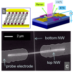
crossed-nwCrossed-nanowire molecular junctions: A new multi-spectroscopy platform for molecular conduction-structure correlations”, H. P. Yoon, M. M. Maitani, O. M. Cabarcos, L. Cai, T. S. Mayer, and D. L. Allara, Nano Letters 10 (8), 2897-2902, 2010.

1. Department of Electrical Engineering, 2. Department of Materials Science and Engineering, and 3.Department of Chemistry, The Pennsylvania State University, University Park, Pennsylvania 16802

ABSTRACT. We report a crossed-nanowire molecular junction array platform that enables direct measurement of current-voltage-temperature characteristics simultaneously with inelastic electron tunneling and Raman vibrational spectra on the same junction. Measurements on dithiol-terminated oligo(phenylene-ethynylene) junctions show both spectroscopies interrogate the gap-confined molecules to reveal distinct molecular features. This versatile platform allows investigation of advanced phenomena such as molecular switching and cooperative effects with the flexible ability to scale both the junction geometries and array sizes.

LINK