
A first-year graduate student, Yu-Lin (Nick) Hsu, won a Student Award at M&M (Microscopy and Microanalysis Conference; https://www.microscopy.org/MandM/2021/). We also congratulate our former graduate student, Kaden Powell, who had initiated this work.
Their project focuses on hybrid metal-halide perovskite solar cells. M&M is the largest international microscopy conference, often having over 1600 attendees. We are so proud of them. We thank our collaborators (Dr. Chongwen Li, Prof. Yanfa Yan at University of Toledo).
- MSA site: https://www.microscopy.org/awards/onsiteawards.cfm
- ECE News: https://www.ece.utah.edu/2021/08/12/ece-students-awarded-for-research-poster/
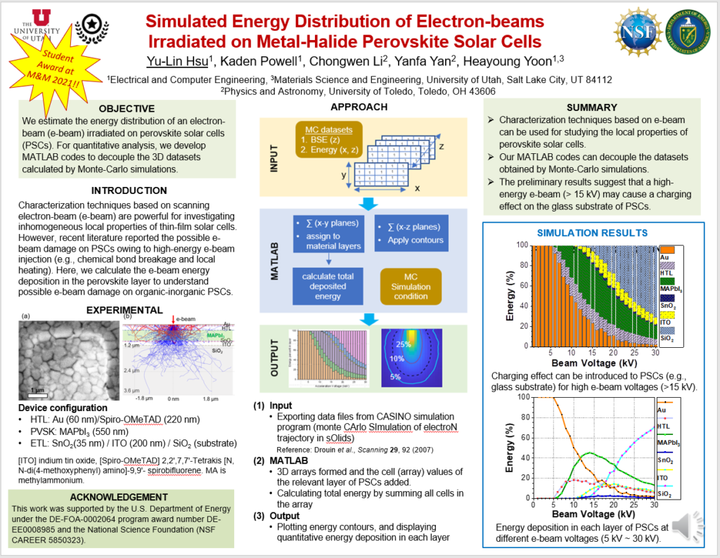
This work was supported by the U.S. Department of Energy under the DE-FOA-0002064 program award number DE-EE0008985 and the National Science Foundation (NSF CAREER 5850323).
 Dr. Yoon is invited to give a talk at the
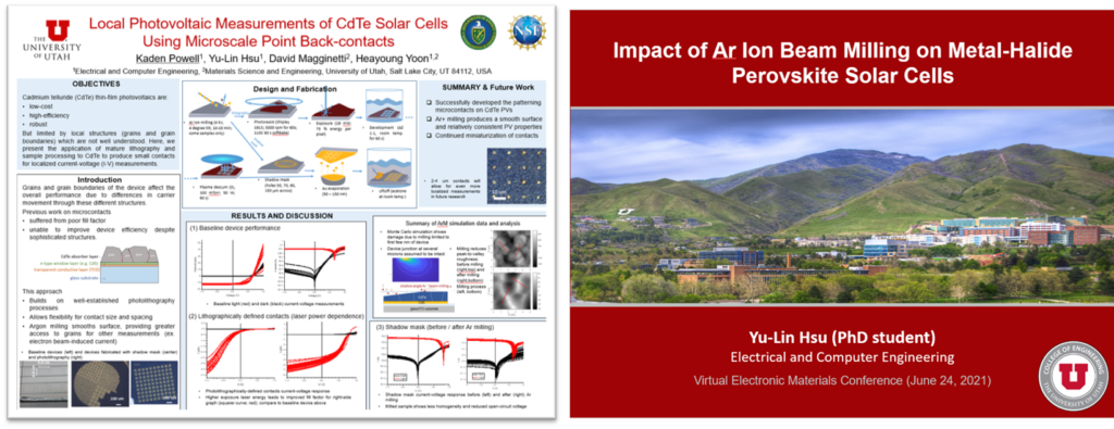
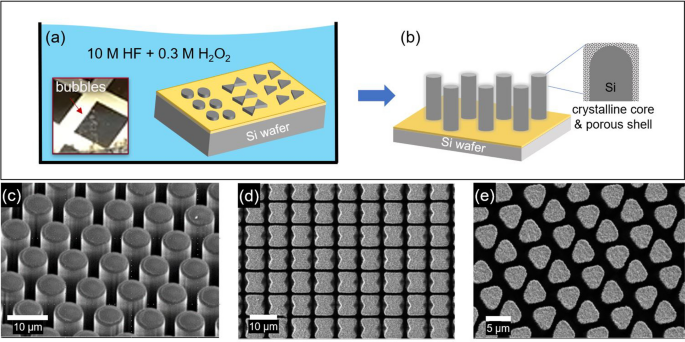
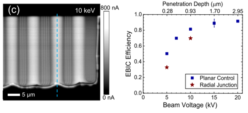 Powell, K.M., Yoon, H.P., “Depth-dependent EBIC microscopy of radial-junction Si micropillar arrays”, Appl. Microsc. 50, 17 (2020).
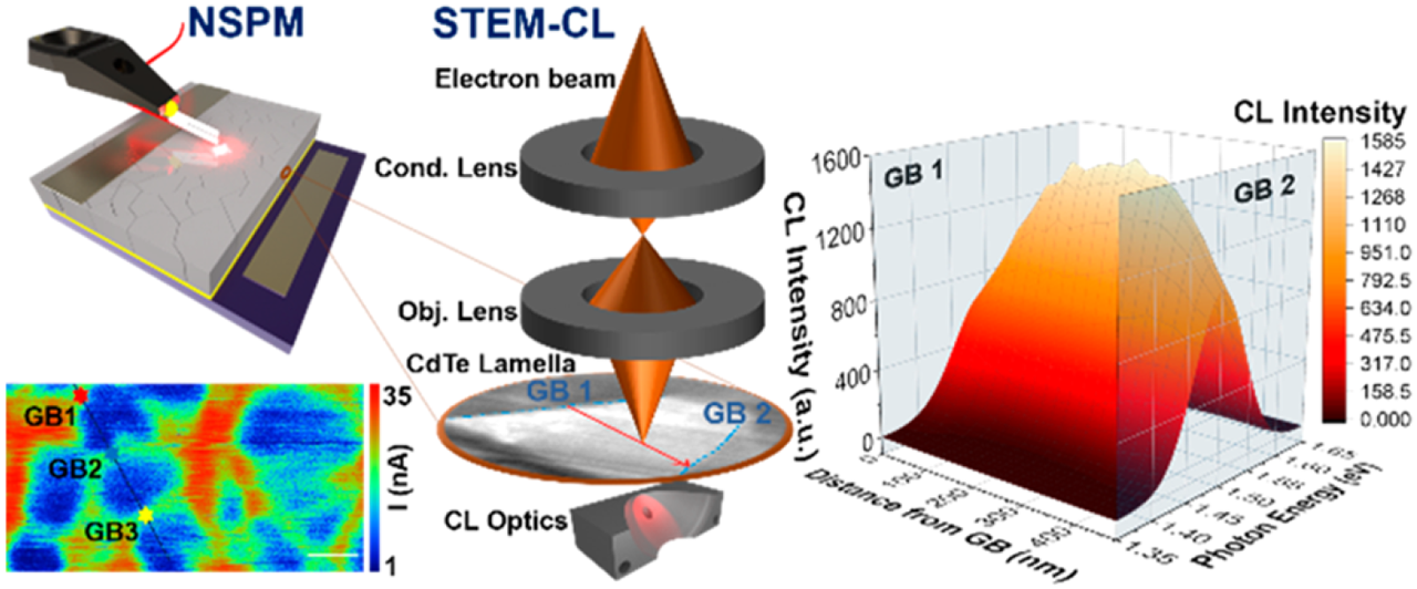
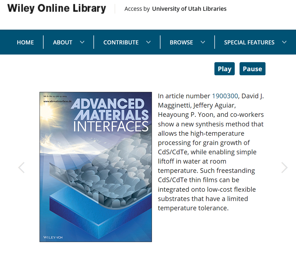
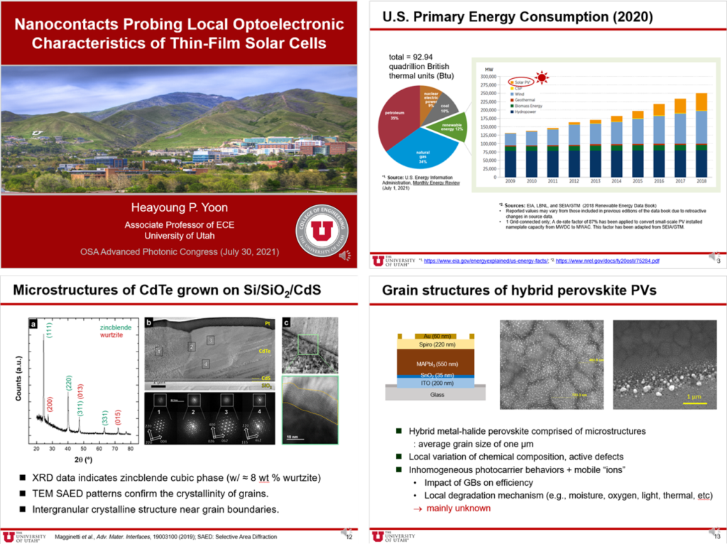
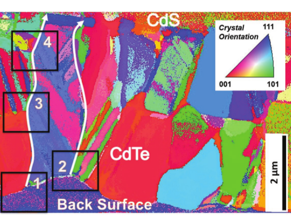 “Observation and Implications of Composition Inhomogeneity Along Grain Boundaries in Thin Film Polycrystalline CdTe Photovoltaic Devices“, S. Misra1, J. A. Aguiar2, Y. Sun3, B. V. Devener2, V. Palekis4, C. S. Ferekides4, H. P. Yoon1, P. Bermel3, M. A. Scarpulla1, Advanced Materials Interfaces 1900152, 2019.