2014 APL Materials

GaNFaceting control in core-shell GaN micropillars using selective epitaxy“, S. Krylyuk, R. Debnath, H. P. Yoon, M. R. King, J. Ha, B. Wen, A. Motayed, and A. V. Davydov, APL Materials 2, 106104, 2014.

1. Materials Science and Engineering Division, National Institute of Standards and Technology, Gaithersburg, Maryland 20899
2. Institute for Research in Electronics and Applied Physics, University of Maryland, College Park, Maryland 20742
3. N5 Sensors, Inc., Rockville, Maryland 20852
4. Center for Nanoscale Science and Technology, National Institute of Standards and Technology, Gaithersburg, Maryland 20899
5. Maryland Nanocenter, University of Maryland, College Park, Maryland 20742
6. Northrop Grumman ES, Linthicum, Maryland 21090

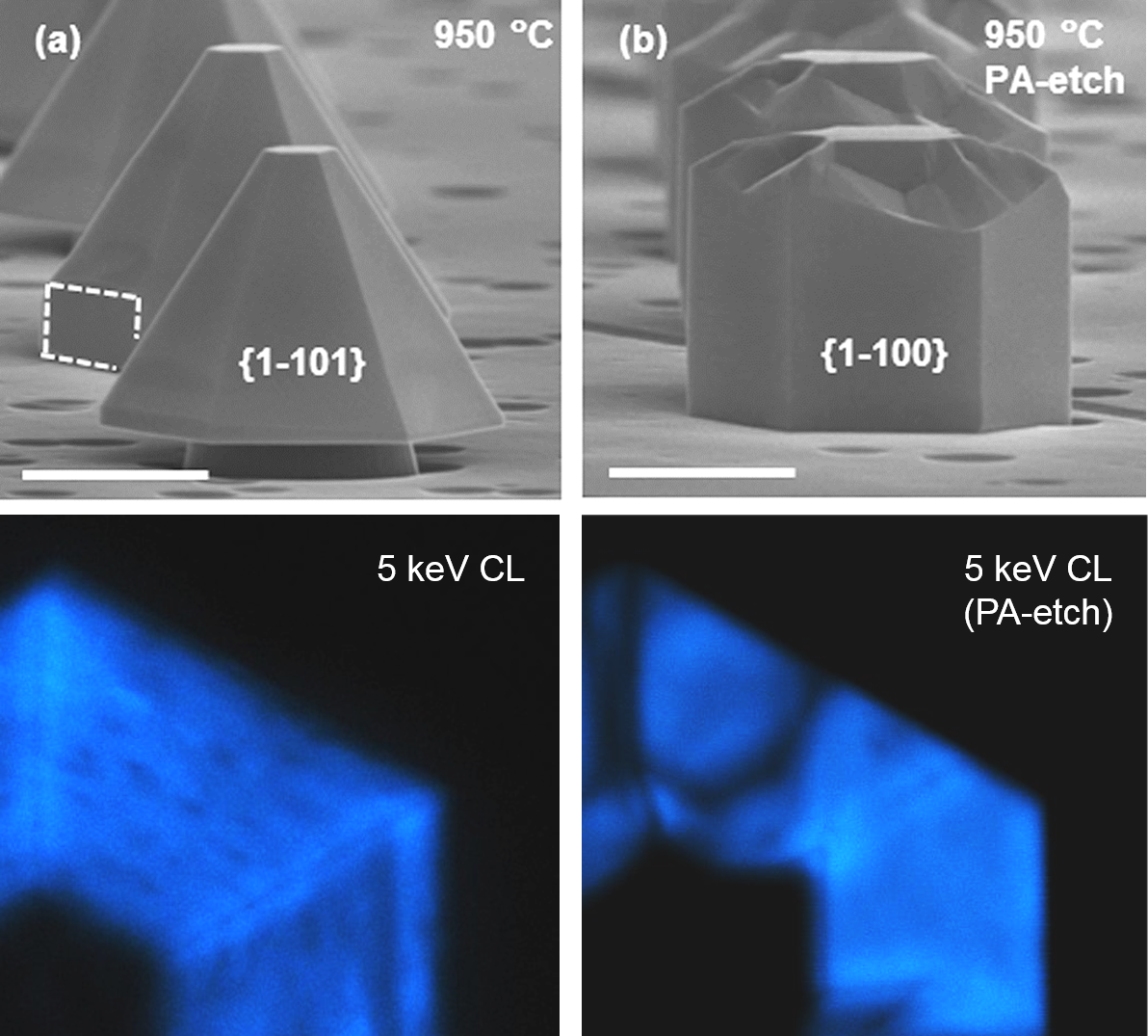
ABSTRACT. We report on the fabrication of large-area, vertically aligned GaN epitaxial core-shell micropillar arrays. The two-step process consists of inductively coupled plasma (ICP) etching of lithographically patterned GaN-on-Si substrate to produce an array of micropillars followed by selective growth of GaN shells over these pillars using Hydride Vapor Phase Epitaxy (HVPE). The most significant aspect of the study is the demonstration of the sidewall facet control in the shells, ranging from {1 1̄ 01} semi-polar to {1 1̄ 00} non-polar planes, by employing a post-ICP chemical etch and by tuning the HVPE growth temperature. Room temperature photoluminescence, cathodoluminescence, and Raman scattering measurements reveal substantial reduction of parasitic yellow luminescence as well as strain-relaxation in the core-shell structures. In addition, X-ray diffraction indicates improved crystal quality after the shell formation. This study demonstrates the feasibility of selective epitaxy on micro-/nano- engineered templates for realizing high-quality GaN-on-Si devices.

LINK

2014 The Society for Information Display

sid2“Cathodoluminescence quantum efficiency of quantum dot thin films”, H. P. Yoon, C. D. Bohn, Y. Lee, S. Ko, J. S. Steckel, S. Coe-Sullivan, N. B. Zhitenev, The Society for Information Display Technical Digests 45, 71–74, 2014.

1. Center for Nanoscale Science and Technology, National Institute of Standards and Technology, Gaithersburg, MD 20899, United States
2. Maryland Nanocenter, University of Maryland, College Park, MD 20742, United States
3. QD Vision Inc., 29 Hartwell Ave., Lexington, MA 02421, United States

ABSTRACT. A thin film of quantum dots (QD) was used to visualize the local photo-response of polycrystalline CdTe solar cells by downconverting an electron beam of high energy to photons of visible light. The efficient photon generation in the QD film is compared to cathodoluminescence of the high-purity bulk semiconductors and phosphor.

LINK

2014 7th Annual FIB SEM Workshop

usermeeting
“Effects of Focused-Ion-Beam Processing on Local Measurements of Semiconductor Solar Cells”, H. P. Yoon, P. M. Haney, J. Schumacher, K. Siebein, Y. Yoon, and N. B. Zhitenev, presented by H. Yoon at the 7th Annual FIB SEM Workshop in Laurel, MD, February 2014.

1. Center for Nanoscale Science and Technology, National Institute of Standards and Technology, Gaithersburg, Maryland, 20899, USA. 2. Maryland Nanocenter, University of Maryland, College Park, Maryland, 20742, USA

ABSTRACT. Quantitative determination of electronic properties at high spatial resolution is crucial for the development of high-efficiency solar cells. Electron beam induced current (EBIC) is a powerful technique in which electron-hole pairs are created in proximity to an exposed surface, and the carrier collection efficiency is measured as a function of excitation position. Cross-sections of device are often created by focused ion beams (FIB) due to the flexibility of the patterning and milling processes. However, the irradiating Ga ions of the FIB fabrication may introduce unintended artifacts, affecting local electronic properties. In this talk, we discuss the impact of the FIB process observed in EBIC measurements and two-dimensional finite element simulations. A series of EBIC data was obtained on a single crystalline solar cell at different electron beam voltages and beam currents to examine the depth and carrier injection level dependence inside the depletion region and away from the p-n junction. Quantitative analysis shows that the EBIC efficiency of the FIB sample is much lower (< 40 %) than that of the cleaved sample (100%) at low beam voltages (<10 keV). We discuss the effects of FIB processing of other types of photovoltaic devices including CdTe and CIGS solar cells.

LINK (NDR contents are not presented)

2013 AIP Advances

qebicHigh-resolution photocurrent microscopy using near-field cathodoluminescence of quantum dots”, H. P. Yoon, Y. Lee, C. D. Bohn, S. Ko, A. G. Gianfrancesco, J. S. Steckel, S. Coe-Sullivan, A. A. Talin, and N. B. Zhitenev, AIP Advances 3, 062112, 2013.

1. Center for Nanoscale Science and Technology, National Institute of Standards and Technology, Gaithersburg, MD 20899, USA
2. Maryland Nanocenter, University of Maryland, College Park, MD 20742, USA
3. Department of physics, Worcester Polytechnic Institute, Worcester, MA 01602, USA
4. QD Vision Inc., 29 Hartwell Ave., Lexington, MA 02421, USA
5. Sandia National Laboratories, Livermore, CA 94550, USA

ABSTRACT. We report a fast, versatile photocurrent imaging technique to visualize the local photo response of solar energy devices and optoelectronics using near-field cathodoluminescence (CL) from a homogeneous quantum dot layer. This approach is quantitatively compared with direct measurements of high-resolution Electron Beam Induced Current (EBIC) using a thin film solar cell (n-CdS / p-CdTe). Qualitatively, the observed image contrast is similar, showing strong enhancement of the carrier collection efficiency at the p-n junction and near the grain boundaries. The spatial resolution of the new technique, termed Q-EBIC (EBIC using quantum dots), is determined by the absorption depth of photons. The results demonstrate a new method for highresolution, sub-wavelength photocurrent imaging measurement relevant for a wide range of applications.

LINK