2015 Nanotechnology

Paul_NanotechnologyElectron beam induced current in the high injection regime”, P. M. Haney, H. P. Yoon, P. Koirala, R. W. Collins, and N. B. Zhitenev, Nanotechnology 26, 295401, 2015.

1. Center for Nanoscale Science and Technology, National Institute of Standards and Technology, Gaithersburg, MD 20899, USA.
2. Maryland NanoCenter, University of Maryland, College Park, MD 20742.
3. Dept. of Physics and Astronomy, University of Toledo, Toledo, OH, 43606.

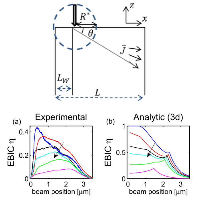
ABSTRACT. Electron beam induced current (EBIC) is a powerful technique which measures the charge collection efficiency of photovoltaics with sub-micron spatial resolution. The exciting electron beam results in a high generation rate density of electron–hole pairs, which may drive the system into nonlinear regimes. An analytic model is presented which describes the EBIC response when the total electron–hole pair generation rate exceeds the rate at which carriers are extracted by the photovoltaic cell, and charge accumulation and screening occur. The model provides a simple estimate of the onset of the high injection regime in terms of the material resistivity and thickness, and provides a straightforward way to predict the EBIC lineshape in the high injection regime. The model is verified by comparing its predictions to numerical simulations in one- and two-dimensions. Features of the experimental data, such as the magnitude and position of maximum collection efficiency versus electron beam current, are consistent with the  three dimensional model.

LINK

2015 IEEE Photovoltaic Specialists Conference

pvsc_2015_posterLocal Photocarrier Dynamics in CdTe Solar Cells Under Optical and Electron Beam Excitations”, H. P. Yoon, P. M. Haney, Y. Yoon, S. An, J. I. Basham, and N. B. Zhitenev, 42th IEEE Photovoltaic Specialists Conference, p. 1, 2015. (DOI: 10.1109/PVSC.2015.7356020)

1. Center for Nanoscale Science and Technology, National Institute of Standards and Technology, Gaithersburg, Maryland, 20899, USA.
2. Maryland Nanocenter, University of Maryland, College Park, Maryland, 20742, USA

ABSTRACT. We compare local carrier dynamics in n-CdS / p-CdTe solar cells, where the electron-hole pairs are generated by either near-field optical illumination or highly focused electron beam excitation. An ion beam milling process was used to prepare a smooth surface of cross-sectional devices. The spatially resolved photocurrent images confirm high carrier collection efficiency at grain boundaries. An analytical model was used to extract material parameters at the level of single grains. We find that the minority carrier diffusion lengths extracted from both local measurement techniques are in excellent agreement, but are smaller than the values determined from macro-scale measurements.

LINK

2014 Microscopy and Microanalysis

MandMEffects of Focused-Ion-Beam Processing on Local Electrical Measurements of Inorganic Solar Cells“, H. P. Yoon, P. M. Haney, J. Schumacher, K. Siebein, Y. Yoon, and N. B. Zhitenev, Microscopy and Microanalysis 20 (S3), 544-545, 2014.

1.Center for Nanoscale Science and Technology, National Institute of Standards and Technology, Gaithersburg, MD 20899, USA
2. Maryland Nanocenter, University of Maryland, College Park, MD 20742, USA

ABSTRACT. Quantitative determination of electronic properties at high spatial resolution is crucial for the development of high-efficiency solar cells. Electron beam induced current (EBIC) is a powerful technique in which electron-hole pairs are created in proximity to an exposed surface, and the carrier collection efficiency is measured as a function of excitation position. Cross-sections of device are often created by focused ion beams (FIB) due to the flexibility of the patterning and milling processes. However, the irradiating Ga ions of the FIB fabrication may introduce unintended artifacts, affecting local electronic properties. In this study, we investigate the impact of the FIB process observed in EBIC measurements and two-dimensional finite element simulations.

LINK

2014 Progress in Photovoltaics

pip_epi_EBIC“Comparison of thin epitaxial film silicon photovoltaics fabricated on monocrystalline and polycrystalline seed layers on glass”, C. W. Teplin, S. Grover, A. Chitu, A. Limanov, M. Chalal, J. Im, D. Amkreutz, S. Gall, H. P. Yoon, V. Lasalvia, H. M. Branz, P. Stradins, K. M. Jones, A. G. Norman, D. L. Young, B. Lee, Progress in Photovoltaics, in press (DOI: 10.1002/pip.2505), 2014.

1. National Renewable Energy Laboratory, Golden, CO, USA
2. Columbia University, New York, NY, USA
3. Helmholtz Zentrum Berlin für Materialien und Energie, Berlin, Germany
4. Center for Nanoscale Science and Technology, National Institute of Standards and Technology, Gaithersburg, MD 20899, USA

ABSTRACT:  We fabricate thin epitaxial crystal silicon solar cells on display glass and fused silica substrates overcoated with a silicon seed layer. To confirm the quality of hot-wire chemical vapor deposition epitaxy, we grow a 2-μm-thick absorber on a (100) monocrystalline Si layer transfer seed on display glass and achieve 6.5% efficiency with an open circuit voltage (V_OC) of 586mV without light-trapping features. This device enables the evaluation of seed layers on display glass. Using polycrystalline seeds formed from amorphous silicon by laser-induced mixed phase solidification (MPS) and electron beam crystallization, we demonstrate 2.9%, 476mV (MPS) and 4.1%, 551mV (electron beam crystallization) solar cells. Grain boundaries likely limit the solar cell grown on the MPS seed layer, and we establish an upper bound for the grain boundary recombination velocity (S_GB) of 1.6×104 cm/s.

LINK

2014 The Society for Information Display

sid2“Cathodoluminescence quantum efficiency of quantum dot thin films”, H. P. Yoon, C. D. Bohn, Y. Lee, S. Ko, J. S. Steckel, S. Coe-Sullivan, N. B. Zhitenev, The Society for Information Display Technical Digests 45, 71–74, 2014.

1. Center for Nanoscale Science and Technology, National Institute of Standards and Technology, Gaithersburg, MD 20899, United States
2. Maryland Nanocenter, University of Maryland, College Park, MD 20742, United States
3. QD Vision Inc., 29 Hartwell Ave., Lexington, MA 02421, United States

ABSTRACT. A thin film of quantum dots (QD) was used to visualize the local photo-response of polycrystalline CdTe solar cells by downconverting an electron beam of high energy to photons of visible light. The efficient photon generation in the QD film is compared to cathodoluminescence of the high-purity bulk semiconductors and phosphor.

LINK

2014 7th Annual FIB SEM Workshop

usermeeting
“Effects of Focused-Ion-Beam Processing on Local Measurements of Semiconductor Solar Cells”, H. P. Yoon, P. M. Haney, J. Schumacher, K. Siebein, Y. Yoon, and N. B. Zhitenev, presented by H. Yoon at the 7th Annual FIB SEM Workshop in Laurel, MD, February 2014.

1. Center for Nanoscale Science and Technology, National Institute of Standards and Technology, Gaithersburg, Maryland, 20899, USA. 2. Maryland Nanocenter, University of Maryland, College Park, Maryland, 20742, USA

ABSTRACT. Quantitative determination of electronic properties at high spatial resolution is crucial for the development of high-efficiency solar cells. Electron beam induced current (EBIC) is a powerful technique in which electron-hole pairs are created in proximity to an exposed surface, and the carrier collection efficiency is measured as a function of excitation position. Cross-sections of device are often created by focused ion beams (FIB) due to the flexibility of the patterning and milling processes. However, the irradiating Ga ions of the FIB fabrication may introduce unintended artifacts, affecting local electronic properties. In this talk, we discuss the impact of the FIB process observed in EBIC measurements and two-dimensional finite element simulations. A series of EBIC data was obtained on a single crystalline solar cell at different electron beam voltages and beam currents to examine the depth and carrier injection level dependence inside the depletion region and away from the p-n junction. Quantitative analysis shows that the EBIC efficiency of the FIB sample is much lower (< 40 %) than that of the cleaved sample (100%) at low beam voltages (<10 keV). We discuss the effects of FIB processing of other types of photovoltaic devices including CdTe and CIGS solar cells.

LINK (NDR contents are not presented)

2013 Solar Energy Materials and Solar Cells

solmat_CdTeLocal electrical characterization of cadmium telluride solar cells using low-energy electron beam”, H. P. Yoon, P. M. Haney, D. Ruzmetov, H. Xu, B. H. Hamadani, A. A. Talin, and N. B. Zhitenev, Solar Energy Materials and Solar Cells 117, 499-504, 2013.

1. Center for Nanoscale Science and Technology, National Institute of Standards and Technology, Gaithersburg, MD 20899.
2. Energy and Environment Division, National Institute of Standards and Technology, Gaithersburg, Maryland, 20899, USA.
3. Maryland Nanocenter, University of Maryland, College Park, MD 20742, USA

ABSTRACT. We investigate local electronic properties of cadmium telluride solar cells using electron beam induced current (EBIC) measurements with patterned contacts. EBIC measurements are performed with a spatial resolution as high as ≈20 nm both on the top surface and throughout the cross-section of the device, revealing an enhanced carrier collection in the vicinity of grain boundaries. Furthermore, we measure local current-voltage characteristics using contacts with dimension both larger (≈5 µm × 10 µm) and smaller (≈1 µm × 1 µm) than the device thickness (≈4 µm), finding that the value of local open-circuit voltage is also larger near grain boundaries.

LINK

2013 AIP Advances

qebicHigh-resolution photocurrent microscopy using near-field cathodoluminescence of quantum dots”, H. P. Yoon, Y. Lee, C. D. Bohn, S. Ko, A. G. Gianfrancesco, J. S. Steckel, S. Coe-Sullivan, A. A. Talin, and N. B. Zhitenev, AIP Advances 3, 062112, 2013.

1. Center for Nanoscale Science and Technology, National Institute of Standards and Technology, Gaithersburg, MD 20899, USA
2. Maryland Nanocenter, University of Maryland, College Park, MD 20742, USA
3. Department of physics, Worcester Polytechnic Institute, Worcester, MA 01602, USA
4. QD Vision Inc., 29 Hartwell Ave., Lexington, MA 02421, USA
5. Sandia National Laboratories, Livermore, CA 94550, USA

ABSTRACT. We report a fast, versatile photocurrent imaging technique to visualize the local photo response of solar energy devices and optoelectronics using near-field cathodoluminescence (CL) from a homogeneous quantum dot layer. This approach is quantitatively compared with direct measurements of high-resolution Electron Beam Induced Current (EBIC) using a thin film solar cell (n-CdS / p-CdTe). Qualitatively, the observed image contrast is similar, showing strong enhancement of the carrier collection efficiency at the p-n junction and near the grain boundaries. The spatial resolution of the new technique, termed Q-EBIC (EBIC using quantum dots), is determined by the absorption depth of photons. The results demonstrate a new method for highresolution, sub-wavelength photocurrent imaging measurement relevant for a wide range of applications.

LINK

2012 IEEE Photovoltaic Specialists Conference

pvsc_ebicHigh-resolution local-current measurement of CdTe solar cells”, H. P. Yoon, D. Ruzmetov, P. M. Haney, B. H. Hamadani, A. A. Talin, N. B. Zhitenev, 38th IEEE Photovoltaic Specialists Conference, pp. 3217-3219, 2012.

1. Center for Nanoscale Science and Technology, National Institute of Standards and Technology, Gaithersburg, Maryland, 20899, USA.
2. Energy and Environment Division, National Institute of Standards and Technology, Gaithersburg, Maryland, 20899, USA
3. Maryland Nanocenter, University of Maryland, College Park, Maryland, 20742, USA

ABSTRACT. We investigate local electronic properties of CdTe solar cells using electron beam to excite electron-hole pairs and evaluate spatially resolved photocurrent characteristics. Standard semiconductor processes were used to fabricate Ohmic metal contacts on the surface of p-type CdTe / n-type CdS device extracted from a commercial solar panel. An ion milling process was used to prepare cross-sections of the devices. Local injection of carriers was controlled by an acceleration voltage of electron beam (1 kV to 30 kV) in a scanning electron microscope, and the
results were correlated with the local morphology, microstructure, and chemical composition of the devices.

LINK