 “Comparison of thin epitaxial film silicon photovoltaics fabricated on monocrystalline and polycrystalline seed layers on glass”, C. W. Teplin, S. Grover, A. Chitu, A. Limanov, M. Chalal, J. Im, D. Amkreutz, S. Gall, H. P. Yoon, V. Lasalvia, H. M. Branz, P. Stradins, K. M. Jones, A. G. Norman, D. L. Young, B. Lee, Progress in Photovoltaics, in press (DOI: 10.1002/pip.2505), 2014.
1. National Renewable Energy Laboratory, Golden, CO, USA
2. Columbia University, New York, NY, USA
3. Helmholtz Zentrum Berlin für Materialien und Energie, Berlin, Germany
4. Center for Nanoscale Science and Technology, National Institute of Standards and Technology, Gaithersburg, MD 20899, USA
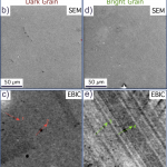
ABSTRACT: We fabricate thin epitaxial crystal silicon solar cells on display glass and fused silica substrates overcoated with a silicon seed layer. To confirm the quality of hot-wire chemical vapor deposition epitaxy, we grow a 2-μm-thick absorber on a (100) monocrystalline Si layer transfer seed on display glass and achieve 6.5% efficiency with an open circuit voltage (V_OC) of 586mV without light-trapping features. This device enables the evaluation of seed layers on display glass. Using polycrystalline seeds formed from amorphous silicon by laser-induced mixed phase solidification (MPS) and electron beam crystallization, we demonstrate 2.9%, 476mV (MPS) and 4.1%, 551mV (electron beam crystallization) solar cells. Grain boundaries likely limit the solar cell grown on the MPS seed layer, and we establish an upper bound for the grain boundary recombination velocity (S_GB) of 1.6×104 cm/s.

