 “Effects of Focused-Ion-Beam Processing on Local Electrical Measurements of Inorganic Solar Cells“, H. P. Yoon, P. M. Haney, J. Schumacher, K. Siebein, Y. Yoon, and N. B. Zhitenev, Microscopy and Microanalysis 20 (S3), 544-545, 2014.
1.Center for Nanoscale Science and Technology, National Institute of Standards and Technology, Gaithersburg, MD 20899, USA
2. Maryland Nanocenter, University of Maryland, College Park, MD 20742, USA
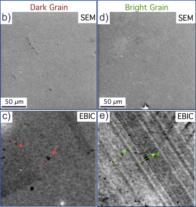
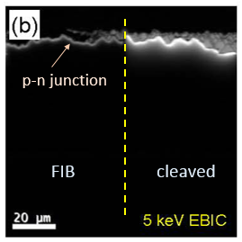
ABSTRACT. Quantitative determination of electronic properties at high spatial resolution is crucial for the development of high-efficiency solar cells. Electron beam induced current (EBIC) is a powerful technique in which electron-hole pairs are created in proximity to an exposed surface, and the carrier collection efficiency is measured as a function of excitation position. Cross-sections of device are often created by focused ion beams (FIB) due to the flexibility of the patterning and milling processes. However, the irradiating Ga ions of the FIB fabrication may introduce unintended artifacts, affecting local electronic properties. In this study, we investigate the impact of the FIB process observed in EBIC measurements and two-dimensional finite element simulations.