Two papers were accepted for oral presentation at EMC in June 2019. Good job, David and Erfan!
Author: HPY
2019 01 Welcome Katrina!
We welcome Katrina Le, a first-year undergrad student (ACCESS Program). She will be working with David to run photovoltaic measurements outside.
2019 01 Invention Disclosure by David and Dr. Yoon.
David and Dr. Yoon have filed an invention discloser related to free-standing optoelectronic thin-film materials. David’s persistence made this happen. Thank you, David!
2018 12 Poster Presentation (eMicroscopy class)
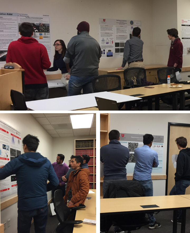
Graduate students in the ECE 6960-006 (eMicroscopy) gave a poster presentation, a part of final project. This interdisciplinary course provides the fundamental knowledge about the (scanning) electron microscopy and the practical lab sessions at the Utah’s Nanofab. The poster session was open to public. Students, thank you for all your hard work!

High resolution SEM imaging of transverse tensile cracks in polymer matrix composites (Caitlin Arndt, Mechanical Engineering)
SEM Porosity characterization of the Jurassic Pimienta Formation (Carlos Vega-Ortiz, Chemical Engineering)
Nanostructure of Cu2O Nanofiber (Karthikeyan Baskaran, Materials Science Engineering)
A look at Resistive RAM (Patsy Cdareanu, Electrical and Computer Engineering)
Electron Microscopy Investigations of asphaltenes precipitation with inorganic solids (Weiyi Kong, Chemical Engineering)
GaN Neutron Radiation (Sam Sprawls, Electrical and Computer Engineering)
2018 12 Army Research Lab visits the U.
The Army Research Lab visited the University of Utah. Dr. Yoon and David attended the technical sessions and provided a lab tour to the program managers. We also discussed the recent development on integrated solar cells.
2018 11 Video Tutorial (e-beam simulator; PART 2)
Second video tutorial for Monte Carlo Simulation of Electron Trajectory in Solid, taught by Dean Collett.
2018 10 CdTe PV Workshop in Toledo, OH
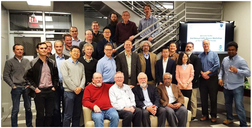
Dr. Yoon attended the 2nd PV workshop and gave two talks. The focus of the workshop is to initiate a closer research community and identification of opportunities for collaborative research, specifically in CdTe.

2018 09 Popular SEM demo by David (Global Class Program)
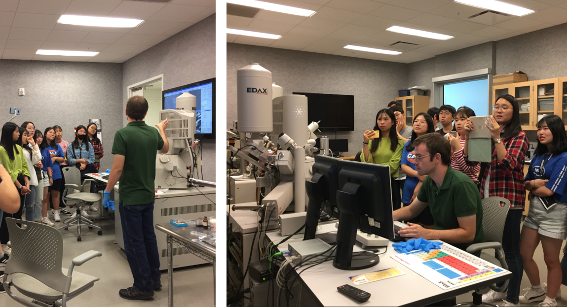
 We welcome Neugju high-school students visiting the University of Utah (Global Engagement Program). David Magginetti (PhD student in Yoon’s group) gave a brief introduction and a demo on scanning electron microscope (SEM). We looked at a coin (10 won) to find a secrete feature in the middle of the pagoda (DaBoTap). Ask students from Neungju High School (South Korea) what they found!
2018 09 Invited Talks at the Regional Workshops
Dr. Yoon attended the regional workshops and gave a talk on an integrated PV system.
- RF and Wireless Day (September 12, Utah State University)
- Advancing the Development Cycle Through Intelligent Materials Design, Informatics, and Characterization (September 6, Colorado School of Mines)
2018 08 Microscopy and Microanalysis (M&M) Conference

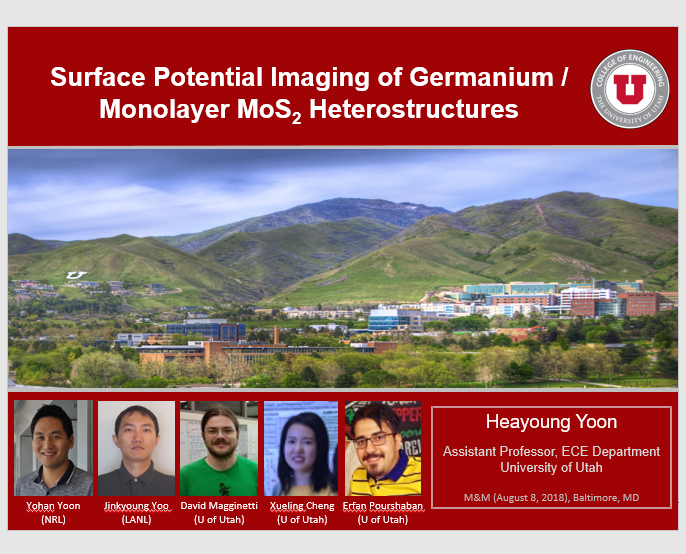
A collaborative work with NIST (National Institute of Standards and Technology) and LANL (Los Alamos National Laboratory) was presented at the M&M conference (Baltimore, MD).
https://doi.org/10.1017/S1431927618008498

