
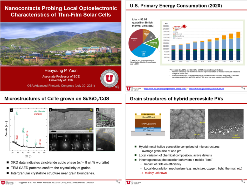
 Dr. Yoon is invited to give a talk at the Advanced Photonics Congress (OSA, The Optical Society) in July, 2021. She will discuss the recent progress on the “Nanocontact Approach” for thin-film photovoltaic materials and devices (CdTe, perovskites).
Publications
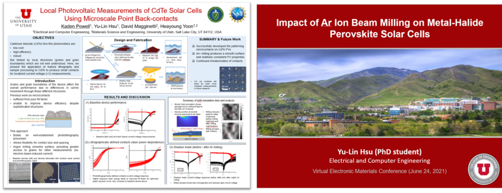
2021 06 EMC Presentation (Kaden, Nick)
Kaden and Nick gave a presentation at the Electronic Materials Conference (EMC). The EMC was held online owing to the COVID situation. Thank you for your work.
2020 10 Publish a Journal Paper (MACE Pillars)
Yang/David’s paper is online now (Scientific Reports). Thank you for their dedication. We also thank to our collaborators.
Yang Qian, David J. Magginetti, Seokmin Jeon, Yohan Yoon, Tony L. Olsen, Maoji Wang, Jordan M. Gerton & Heayoung P. Yoon, “Heterogeneous optoelectronic characteristics of Si micropillar arrays fabricated by metal-assisted chemical etching”, Scientific Reports 10, 16349 (2020)
https://www.nature.com/articles/s41598-020-73445-x
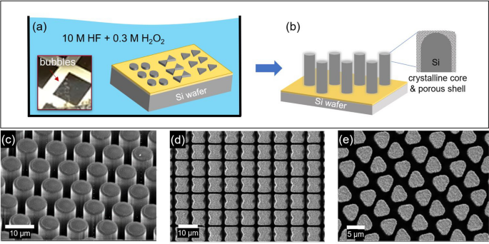
2020 09 Applied Microscopy (DRIE Si Pillars)
Kaden’s first paper has been published. Congratulations!
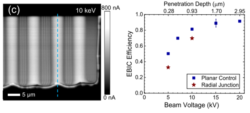 Powell, K.M., Yoon, H.P., “Depth-dependent EBIC microscopy of radial-junction Si micropillar arrays”, Appl. Microsc. 50, 17 (2020).
https://doi.org/10.1186/s42649-020-00037-4 (here)
2019 12 ACS Applied Materials & Interfaces
Our Collaborative work with NIST and NRL is presented in an ACS paper.
“Unveiling Defect-Mediated Charge-Carrier Recombination at the Nanometer Scale in Polycrystalline Solar Cells”, Yohan Yoon, Wei-Chang D. Yang*, Dongheon Ha, Paul M. Haney, Daniel Hirsch, Heayoung P. Yoon, Renu Sharma, and Nikolai B. Zhitenev, ACS Appl. Mater. Interfaces 2019, 11, 50, 47037–47046 (2019); https://pubs.acs.org/doi/full/10.1021/acsami.9b14730
2019 08 Microscopy and Microanalysis Conference
David, Dr. Aguiar, and Dr. Yoon present the development of lightweight and flexible CdTe PVs at the M&M conference (Portland, OR).
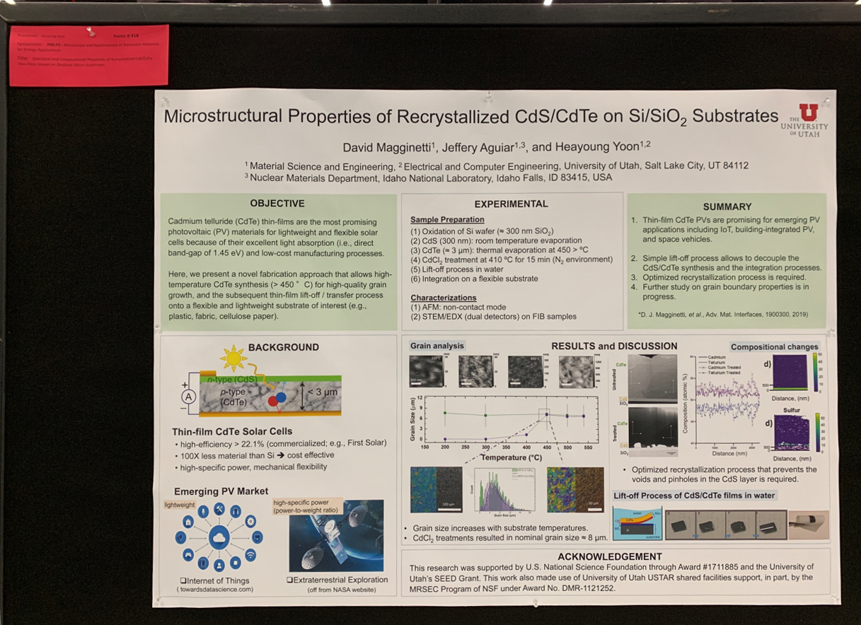
2019 08 Cover (Advanced Materials Interfaces)
David’s paper is selected as cover for Advanced Materials Interfaces. Congratulations, David.
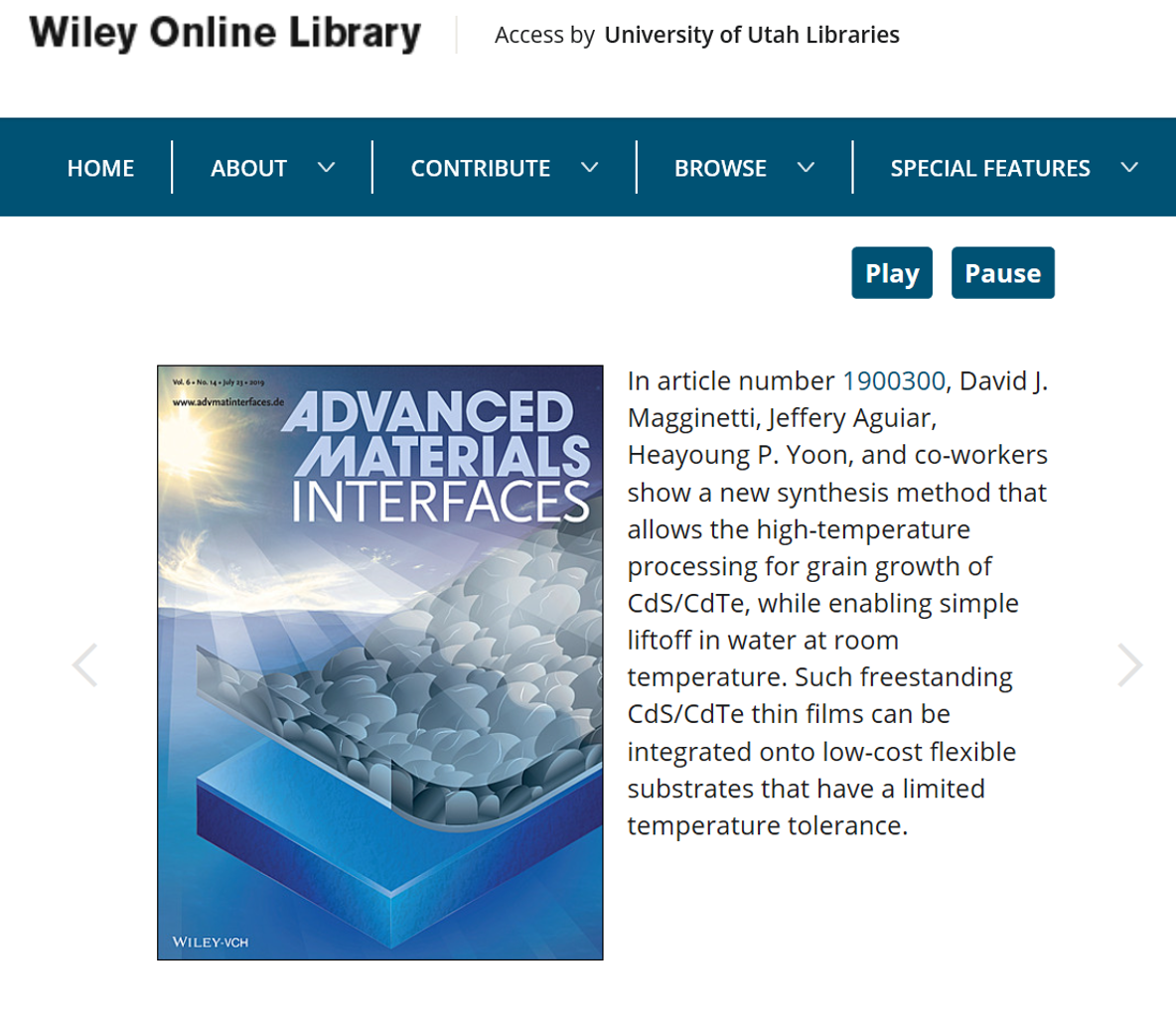
2019 07 Advanced Materials Interfaces
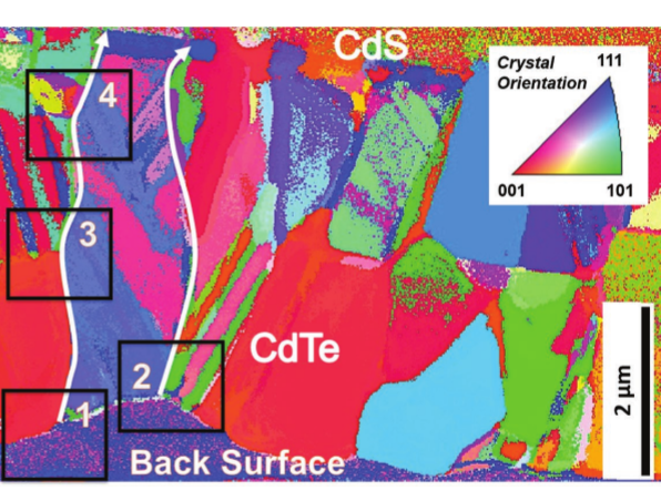 “Observation and Implications of Composition Inhomogeneity Along Grain Boundaries in Thin Film Polycrystalline CdTe Photovoltaic Devices“, S. Misra1, J. A. Aguiar2, Y. Sun3, B. V. Devener2, V. Palekis4, C. S. Ferekides4, H. P. Yoon1, P. Bermel3, M. A. Scarpulla1, Advanced Materials Interfaces 1900152, 2019.
1. Electrical and Computer Engineering, University of Utah, Salt Lake City, UT 84102, USA
2. Nuclear Materials Department, Idaho National Laboratory, Idaho Falls, ID 83415, USA
3. Electrical and Computer Engineering, Purdue University, West Lafayette, IN 47906, USA
4. Electrical Engineering, University of South Florida, Tampa, FL 33620, USA
2019 07 Electronic Materials Conference
Yoon’s group presented two research projects at the 61st Electronic Materials Conference (June 26 ~ June 28, 2019; University of Michigan, Ann Arbor, MI)
♦ Impact of Ar Ion Beam Milling on Surface Properties of Polycrystalline CdTe Solar Cells (David Magginetti, Seokmin Jeon, Yohan Yoon, Erfan Pourshaban, and Heayoung Yoon)
1. Materials Science and Engineering, University of Utah, Salt Lake City, UT 84112, USA
2. U.S. Naval Research Laboratory, Washington, DC 20375, USA
3. Electrical and Computer Engineering, University of Utah, Salt Lake City, UT 84112, USA
♦ Surface Potential Imaging of High-Aspect-Ratio Si Microwires Fabricated by Metal-assisted Chemical Etching Process (Erfan Pourshaban, Seokmin Jeon, Yohan Yoon, David Magginetti, and Heayoung Yoon)
1. Electrical and Computer Engineering, University of Utah, Salt Lake City, UT 84112, USA
2. U.S. Naval Research Laboratory, Washington, DC 20375, USA
3. Materials Science and Engineering, University of Utah, Salt Lake City, UT 84112, USA
2019 05 Advanced Materials Interfaces
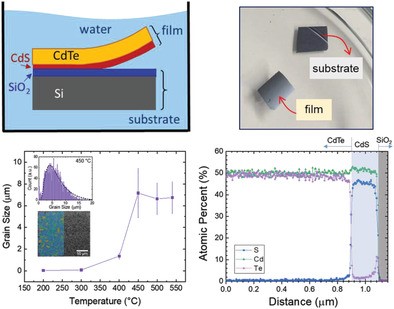 “Water‐Assisted Liftoff of Polycrystalline CdS/CdTe Thin Films Using Heterogeneous Interfacial Engineering“, D. Magginetti1, J. Aguiar1,2, J. Winger1, M. Scarpulla1,3, E. Pourshaban2, H. Yoon1,3, Advanced Materials Interfaces 1900300, 2019.
1. Materials Science and Engineering, University of Utah, Salt Lake City, UT 84102, USA
2. Nuclear Materials Department, Idaho National Laboratory, Idaho Falls, ID 83415, USA
3. Electrical and Computer Engineering, University of Utah, Salt Lake City, UT 84102, USA