A collaborative work with NIST (National Institute of Standards and Technology) and LANL (Los Alamos National Laboratory) was presented at the M&M conference (Baltimore, MD).
https://doi.org/10.1017/S1431927618008498

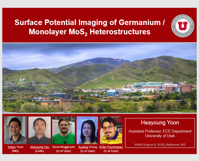
Yoon Research Group (ECE, University of Utah)
A collaborative work with NIST (National Institute of Standards and Technology) and LANL (Los Alamos National Laboratory) was presented at the M&M conference (Baltimore, MD).
https://doi.org/10.1017/S1431927618008498
Yoon’s group presented two research projects at the 60th EMC conference (June 27 ~ June 29, 2018; University of California, Santa Barbara, CA)
♦ Large-area MoTe2 Film Growth Using High-Vacuum Ampoule Process (David Magginetti, Xueling Cheng, Prashanth Gopalan, BerardiSensale-Rodriguez, and Heayoung Yoon)
♦ Local Photovoltage / NSOM Imaging of ZnTe/CdTe Back Contact (Yohan Yoon, David Magginetti, Erfan Pourshaban, Vasilios Palekis, Chih An Hsu, Mike Scarpulla, Chris Ferekides, and Heayoung Yoon)
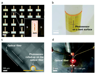 “Wide-spectral/dynamic-range skin-compatible phototransistors enabled by floated heterojunction structures with surface functionalized SWCNTs and amorphous oxide semiconductors“, I. Hwang1, J. Kim1, M. Lee2, M. Lee1, H. Kim1, H. Kwon1, D. Hwang3, M. Kim4, H. Yoon5, Y. Kim2, and S. Park1, Nanoscale 9, 16711, 2017.
1. School of Electrical and Electronics Engineering, Chung-Ang University, Seoul 06974, Korea
2. School of Advanced Materials Science and Engineering and SKKU Advanced Institute of Nanotechnology (SAINT), Sungkyunkwan University, Suwon, Korea
3. Center for Opto-Electronic Materials and Devices, Post-Silicon Semiconductor Institute, Korea Institute of Science and Technology (KIST), Seoul, Korea
4. Department of Chemistry, Chung-Ang University, Seoul, Korea
5. Department of Electrical and Computer Engineering, University of Utah, Salt Lake City, USA
Read more
Dean’s EMC conference paper is accepted for a platform presentation at the 59th EMC Conference (June 28-30, 2017; University of Notre Dame, South Bend, ID).
2017 07 * Dean gives a presentation at the International Conference (EMC).
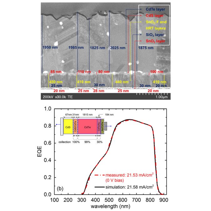
Heterojunction Electronic Properties and Compositional Differences of CdCl2 Post-Treated CdTe Solar Cell (Dean Collett 1, Jeffery A. Aguiar 2,3, Brian v. Devener 4, Yohan Yoon 5,6, Paul Haney 6, Nikolai Zhitenev 6, Michael Scarpulla 1,3, Prakash Koirala 7, Robert W. Collins 7 and Heayoung Yoon 1).
1. Electrical and Computer Engineering, University of Utah, Salt Lake City, Utah.
2. Fuel Design and Development Department, Idaho National Laboratory, Idaho Falls, Idaho.
3. Department of Materials Science and Engineering, University of Utah, Salt Lake City, Utah.
4. Utah Nanofab, University of Utah, Salt Lake City, Utah.
5. Maryland NanoCenter, University of Maryland, College Park, Maryland.
6. Center for Nanoscale Science and Technology, National Institute of Standards and Technology, Gaithersburg, Maryland.
7. Department of Physics and Astronomy, Center for Photovoltaics Innovation and Commercialization, University of Toledo, Toledo, Ohio
Yoon’s group gave a presentation at the Materials Research Society conference. The work is conducted in close collaborations with Dr. Kyu-Bum Han, Dr. Jeffery Aguiar, Dr. Brian van Devener, Prof. Vikram Deshpade, and Prof. Taylor Spark.
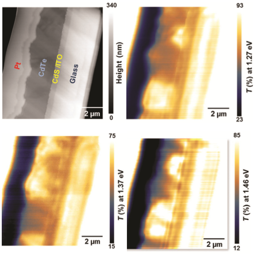
“Nanoscale imaging and spectroscopy of band gap and defects in polycrystalline photovoltaic devices”, Y. Yoon1, 2, J. Chae1, 2, A. M. Katzenmeyer1, H. P. Yoon1,2,3, J. Schumacher1, S. An1, A. Centronea1, and N. Zhitenev1, Nanoscale 9, 7771, 2017.
1. Center for Nanoscale Science and Technology, National Institute of Standards and Technology, Gaithersburg, Maryland 20899, USA;
2. Maryland Nanocenter, College Park, Maryland 02421, USA;
3. Dept. of Electrical & Computer Engineering, University of Utah, Salt Lake City, Utah 84112, USA.
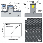 “Deconvoluting the influences of 3D structure on the performance of photoelectrodes for solar-driven water splitting”, D. Esposito1,2, Y. Lee1,3, H. Yoon1,3, P. Haney1, N. Labrador2, T. Moffat1, A. Talin4, and V. Szalai1, Sustainable Energy Fuels 1, 154, 2017.
1. Center for Nanoscale Science and Technology, National Institute of Standards and Technology, Gaithersburg, Maryland 20899, USA;
2. Department of Chemical Engineering, New York, New York 10027, USA;
3. Maryland Nanocenter, College Park, Maryland 02421, USA;
4. Sandia National Laboratories, Livermore, California 94551, USA
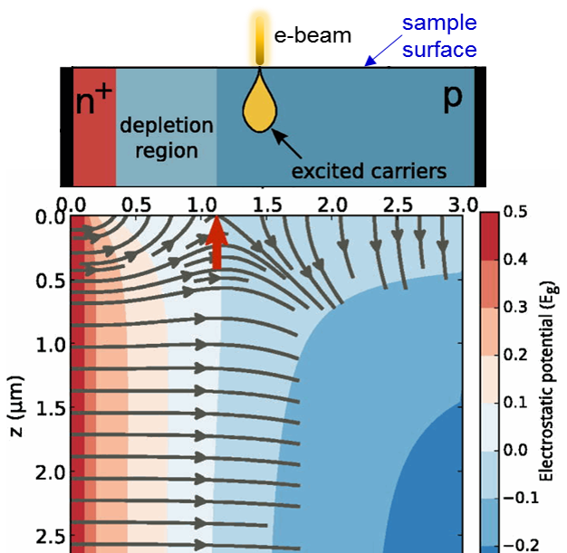 “Depletion region surface effects in electron beam induced current measurements”, P. M. Haney, H. P. Yoon, B. Gaury, and N. B. Zhitenev , J. of Appl. Phys. 120, 105095702, 2016.
1. Center for Nanoscale Science and Technology, National Institute of Standards and Technology, Gaithersburg, Maryland 20899, USA; 2. Department of Electrical and Computer Engineering, University of Utah, Salt Lake City, Utah 84112, USA; 3. Maryland NanoCenter, University of Maryland, College Park, Maryland 20742.
“Imaging Local Optoelectronic Properties of Polycrystalline CdTe Solar Cells”, H. Yoon , Y. Yoon, P. Haney, S. An, P. Koirala, R. Collins, J. Chae, A. Katzenmeyer, A. Centrone and N. Zhitenev, presented by H. Yoon at the Electronic Materials Conference in Newark, DE, June 2016.
1. Electrical and Computer Engineering, University of Utah, Salt Lake City, Utah, USA.
2. Center for Nanoscale Science and Technology, National Institute of Standards and Technology, Gaithersburg, Maryland, USA.
3. Maryland NanoCenter, University of Maryland, College Park, Maryland, USA.
4. Physics and Astronomy, University of Toledo, Toledo, Ohio, USA; 5. Sandia National Laboratories, Albuquerque, New Mexico, USA
 “Through-the-glass spectroscopic ellipsometry for analysis of CdTe thin-film solar cells in the superstrate configuration”, P. Koirala1, J. Li, H. P. Yoon, P. Aryal, S. Marsillac, A. A. Rockett, N. J. Podraza and R. W. Collins, Progress in Photovoltaics 24, 1055, 2016.