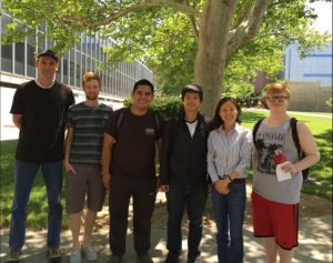
Dr. Yoon presented her research work at the ECE Graduate Seminar on October 17. She also gave an invited talk in the Physics department on October 18.
Author: HPY
Former Group Member
David Magginetti (2020)
David was a graduate RA student. He earned his PhD degree and is currently working at Intel.
“… everyone can reach his goals, if he is able to think, if he is able to wait, if he is able to fast.”
Yang Qian (2020)
Yang was a graduate RA student. She earned her MS degree and left the group for the next journey at the USC.
“Stay positive, work hard, and make it happen.”
Dinorah Segovia (2020)
Dinorah was a undergraduate RA student. She left the group to work in a company in SLC.
“You have not failed until you quit trying.”
Dean Collett (2018)
Dean was a undergraduate RA student. He had left the group to work in the Air Force base in Utah. In 2020, he came back to school (work/study) and is working on his MS degree.
“All effort counts for something. No effort is wasted.”
Yohan Yoon (2017)
Yohan was a post-doc fellow. He left the group for a new research position at Naval Research Laboratory.
Andrew Baker (2017)
Andrew was an REU student from Clarion University. He left the group to continue his BS studies.
“I have no special talents, I am only passionately curious” – A. Einstein
Eric Snyder (2017)
Eric was an undergraduate RA student. He left the group for his PhD study at the University of San-Diego.
“Eric is a father, amateur musician, and an avid reader.”
Zijian Wang (2017)
Zijian was an undergrad RA student. He left the group pursuing a MS degree in other school.
“I like playing the piano and playing soccer. My motto is don’t put off things till tomorrow.”
Alvaro Bonilla (2016)
Alvaro was an undergraduate RA student. He left the group in August 2016 for a position at Holland & Hart.
Austin Koch (2016)
Austin was an REU student from University of Nebraska. He left the group to continue his BS studies.
“I’m a big fan of traveling and love learning languages. I’d love to work on an international level some day.”
Sarah Shipp (2016)
Sarah was an high-school intern in July 2016. Sarah left the group to continue her studies at the Waterford School.
2016 J. of Applied Physics
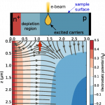 “Depletion region surface effects in electron beam induced current measurements”, P. M. Haney, H. P. Yoon, B. Gaury, and N. B. Zhitenev , J. of Appl. Phys. 120, 105095702, 2016.
1. Center for Nanoscale Science and Technology, National Institute of Standards and Technology, Gaithersburg, Maryland 20899, USA; 2. Department of Electrical and Computer Engineering, University of Utah, Salt Lake City, Utah 84112, USA; 3. Maryland NanoCenter, University of Maryland, College Park, Maryland 20742.
2016 09 * Paper published on EBIC Analysis
 Yoon’s Research group published a journal paper on EBIC (Electron Beam Induced Current) analysis in collaboration with researchers (Dr. Paul Haney, Dr. Benoit Gaury, Dr. Nikolai Zhitenev) in the CNST (Center for Nanoscale Science and Technology) at the National Institute of Standards and Technology.
Paper LINK
2016 09 * Dr. Yoon gives an invited seminar at the LANL.
Dr. Yoon gave an invited seminar on August 31 at the Center for Integrated Nanotechnology in the Los Alamos National Laboratory (Title: Nanoscale EBIC Characterizations of Inhomogeneous Thin Film Solar Cells). Her group will be closely working with the CINT researchers on projects involving nanowires and quantum dots.
2016 08 * Group members receive UROP Awards
Congratulations to Dean Collett, Eric Snyder, and Zijian Wang, who won UROP Awards!
Students from various disciplines around the University of Utah campus write research proposals to compete for the funded research program. UROP (Undergraduate Research Opportunities Program) provides assistantships up to $1,200 for each awardee. More information: http://our.utah.edu/for-students/urop/
2016 08 * REU Poster Presentation
Austin Koch, an REU (Rese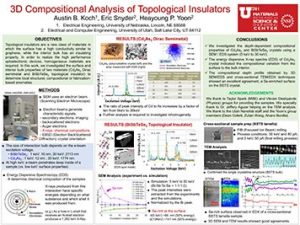 arch Experience for Undergraduates) participant, gave a poster presentation on August 5 at the Chemistry Atrium in Henry Eyring Building. His work focused on the nanoscale compositional analysis of topological insulators and 3D Dirac semimetals.
The samples were provided by Prof. Taylor Sparks (MSE) and Prof. Vikram Deshpande (Physics). The high-resolution STEM/EDX measurements were performed in the Utah Nanofab. Thank for the great help from the TEM experts (Dr. Jeffery Aguiar, Dr. Brian Devener) and Yoon’s Research Group members (Eric Snyder, Alvaro Bonilla, Dean Collett, Zijian, Wang).
Abstract: Topological insulators are a new class of materials in which the surface has a high conductivity similar to graphene, while the interior bulk has an insulating property. In order to realize the high performance optoelectronic devices, homogeneous materials are required. In this work, we investigated the surface and interior bulk properties of two materials (Cd3As2 Dirac semimetal and BiSbTeSe2 topological insulator) to determine local structural, compositional or fabrication-based anomalies.
2016 07 * One Fine Day at the U
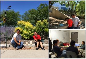 We welcome a high-school intern, Sarah Shipp from the Waterford School. Sarah measures the variation of photocurrent of silicon solar cells that are mounted at 30° and 60° with respect to the ground. Read more
2016 06 * Welcome new group members!
2016 Electronic Materials Conference
“Imaging Local Optoelectronic Properties of Polycrystalline CdTe Solar Cells”, H. Yoon , Y. Yoon, P. Haney, S. An, P. Koirala, R. Collins, J. Chae, A. Katzenmeyer, A. Centrone and N. Zhitenev, presented by H. Yoon at the Electronic Materials Conference in Newark, DE, June 2016.
1. Electrical and Computer Engineering, University of Utah, Salt Lake City, Utah, USA.
2. Center for Nanoscale Science and Technology, National Institute of Standards and Technology, Gaithersburg, Maryland, USA.
3. Maryland NanoCenter, University of Maryland, College Park, Maryland, USA.
4. Physics and Astronomy, University of Toledo, Toledo, Ohio, USA; 5. Sandia National Laboratories, Albuquerque, New Mexico, USA


