2014 The Society for Information Display

sid2“Cathodoluminescence quantum efficiency of quantum dot thin films”, H. P. Yoon, C. D. Bohn, Y. Lee, S. Ko, J. S. Steckel, S. Coe-Sullivan, N. B. Zhitenev, The Society for Information Display Technical Digests 45, 71–74, 2014.

1. Center for Nanoscale Science and Technology, National Institute of Standards and Technology, Gaithersburg, MD 20899, United States
2. Maryland Nanocenter, University of Maryland, College Park, MD 20742, United States
3. QD Vision Inc., 29 Hartwell Ave., Lexington, MA 02421, United States

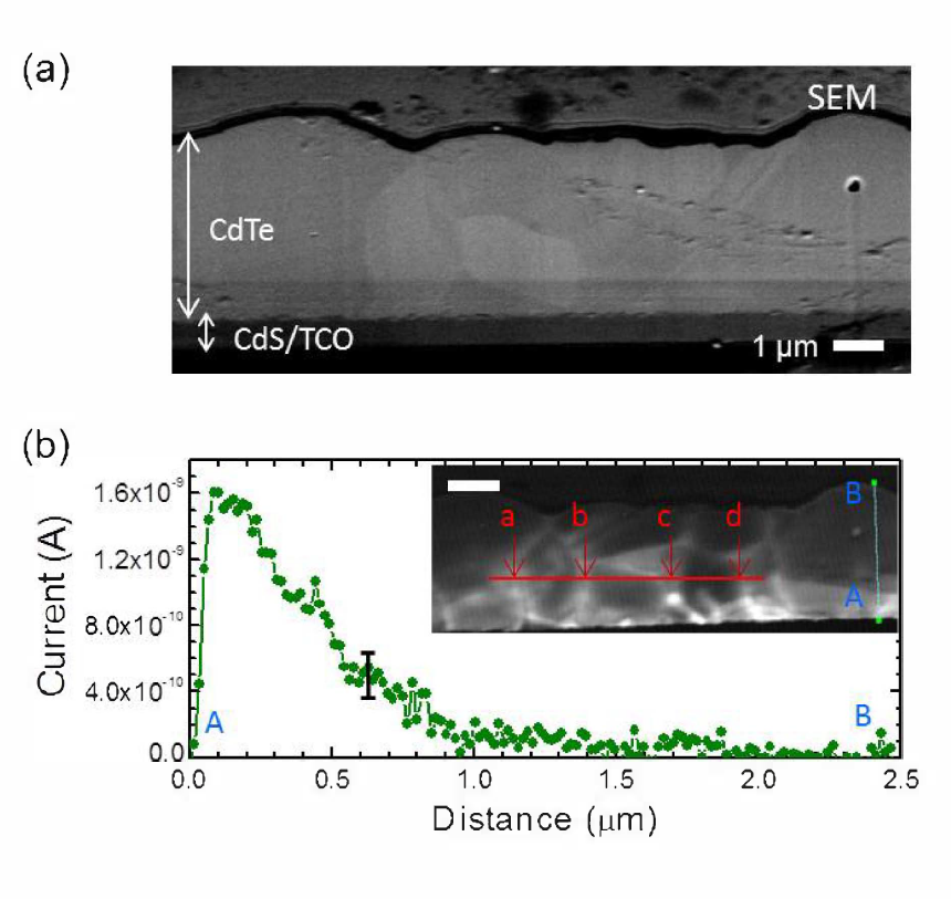
ABSTRACT. A thin film of quantum dots (QD) was used to visualize the local photo-response of polycrystalline CdTe solar cells by downconverting an electron beam of high energy to photons of visible light. The efficient photon generation in the QD film is compared to cathodoluminescence of the high-purity bulk semiconductors and phosphor.

LINK

2014 7th Annual FIB SEM Workshop

usermeeting
“Effects of Focused-Ion-Beam Processing on Local Measurements of Semiconductor Solar Cells”, H. P. Yoon, P. M. Haney, J. Schumacher, K. Siebein, Y. Yoon, and N. B. Zhitenev, presented by H. Yoon at the 7th Annual FIB SEM Workshop in Laurel, MD, February 2014.

1. Center for Nanoscale Science and Technology, National Institute of Standards and Technology, Gaithersburg, Maryland, 20899, USA. 2. Maryland Nanocenter, University of Maryland, College Park, Maryland, 20742, USA

ABSTRACT. Quantitative determination of electronic properties at high spatial resolution is crucial for the development of high-efficiency solar cells. Electron beam induced current (EBIC) is a powerful technique in which electron-hole pairs are created in proximity to an exposed surface, and the carrier collection efficiency is measured as a function of excitation position. Cross-sections of device are often created by focused ion beams (FIB) due to the flexibility of the patterning and milling processes. However, the irradiating Ga ions of the FIB fabrication may introduce unintended artifacts, affecting local electronic properties. In this talk, we discuss the impact of the FIB process observed in EBIC measurements and two-dimensional finite element simulations. A series of EBIC data was obtained on a single crystalline solar cell at different electron beam voltages and beam currents to examine the depth and carrier injection level dependence inside the depletion region and away from the p-n junction. Quantitative analysis shows that the EBIC efficiency of the FIB sample is much lower (< 40 %) than that of the cleaved sample (100%) at low beam voltages (<10 keV). We discuss the effects of FIB processing of other types of photovoltaic devices including CdTe and CIGS solar cells.

LINK (NDR contents are not presented)

2014 Science

mofTunable electrical conductivity in metal-organic framework thin film devices”, A. A. Talin, A. Centrone, M. E. Foster, V. Stavila, P. M. Haney, R. A. Kinney, V. A. Szalai, F. E. Gabaly, H. P. Yoon, F. Léonard, and M. D. Allendorf, Science 343, 66-69, 2014.

1. Sandia National Laboratories, Livermore, CA 94551, USA.
2. Center for Nanoscale Science and Technology, National Institute of Standards and Technology, Gaithersburg, MD 20899, USA.
3. Maryland Nanocenter, University of Maryland, College Park, MD 20742, USA.

ABSTRACT. We report a strategy for realizing tunable electrical conductivity in metal-organic frameworks (MOFs) in which the nanopores are infiltrated with redox-active, conjugated guest molecules. This approach is demonstrated using thin-film devices of the MOF Cu3(BTC)2 (also known as HKUST-1; BTC, benzene-1,3,5-tricarboxylic acid) infiltrated with the molecule 7,7,8,8-tetracyanoquinododimethane (TCNQ). Tunable, air-stable electrical conductivity over six orders of magnitude is achieved, with values as high as 7 siemens per meter. Spectroscopic data and first-principles modeling suggest that the conductivity arises from TCNQ guest molecules bridging the binuclear copper paddlewheels in the framework, leading to strong electronic coupling between the dimeric Cu subunits. These ohmically conducting porous MOFs could have applications in conformal electronic devices, reconfigurable electronics, and sensors.

LINK

2013 Solar Energy Materials and Solar Cells

solmat_CdTeLocal electrical characterization of cadmium telluride solar cells using low-energy electron beam”, H. P. Yoon, P. M. Haney, D. Ruzmetov, H. Xu, B. H. Hamadani, A. A. Talin, and N. B. Zhitenev, Solar Energy Materials and Solar Cells 117, 499-504, 2013.

1. Center for Nanoscale Science and Technology, National Institute of Standards and Technology, Gaithersburg, MD 20899.
2. Energy and Environment Division, National Institute of Standards and Technology, Gaithersburg, Maryland, 20899, USA.
3. Maryland Nanocenter, University of Maryland, College Park, MD 20742, USA

ABSTRACT. We investigate local electronic properties of cadmium telluride solar cells using electron beam induced current (EBIC) measurements with patterned contacts. EBIC measurements are performed with a spatial resolution as high as ≈20 nm both on the top surface and throughout the cross-section of the device, revealing an enhanced carrier collection in the vicinity of grain boundaries. Furthermore, we measure local current-voltage characteristics using contacts with dimension both larger (≈5 µm × 10 µm) and smaller (≈1 µm × 1 µm) than the device thickness (≈4 µm), finding that the value of local open-circuit voltage is also larger near grain boundaries.

LINK

2013 AIP Advances

qebicHigh-resolution photocurrent microscopy using near-field cathodoluminescence of quantum dots”, H. P. Yoon, Y. Lee, C. D. Bohn, S. Ko, A. G. Gianfrancesco, J. S. Steckel, S. Coe-Sullivan, A. A. Talin, and N. B. Zhitenev, AIP Advances 3, 062112, 2013.

1. Center for Nanoscale Science and Technology, National Institute of Standards and Technology, Gaithersburg, MD 20899, USA
2. Maryland Nanocenter, University of Maryland, College Park, MD 20742, USA
3. Department of physics, Worcester Polytechnic Institute, Worcester, MA 01602, USA
4. QD Vision Inc., 29 Hartwell Ave., Lexington, MA 02421, USA
5. Sandia National Laboratories, Livermore, CA 94550, USA

ABSTRACT. We report a fast, versatile photocurrent imaging technique to visualize the local photo response of solar energy devices and optoelectronics using near-field cathodoluminescence (CL) from a homogeneous quantum dot layer. This approach is quantitatively compared with direct measurements of high-resolution Electron Beam Induced Current (EBIC) using a thin film solar cell (n-CdS / p-CdTe). Qualitatively, the observed image contrast is similar, showing strong enhancement of the carrier collection efficiency at the p-n junction and near the grain boundaries. The spatial resolution of the new technique, termed Q-EBIC (EBIC using quantum dots), is determined by the absorption depth of photons. The results demonstrate a new method for highresolution, sub-wavelength photocurrent imaging measurement relevant for a wide range of applications.

LINK

2013 Chemical Communications

ChemCommQuantum dot-DNA origami binding: A single particle, 3D, real-time tracking study”, K. Du, S. Ko, G. M. Gallatin, H. P. Yoon, J. A. Liddle, and A. J. Berglund, Chemical Communications 49, 909-909, 2013

1. Center for Nanoscale Science and Technology, National Institute of Standards and  Technology, Gaithersburg, MD 20899, USA.
2. Maryland Nanocenter, University of Maryland, College Park, MD 20742, USA

ABSTRACT. The binding process of quantum dots and DNA origami was monitored using a 3D, real-time, single-particle tracking system. Single-molecule binding events were directly observed and precise measurements of the diffusion coefficient and second-order photon correlation function, g2(s), were combined to distinguish free quantum dots from different conjugates of nQdot-origami.

LINK

2012 IEEE Photovoltaic Specialists Conference

pvsc_ebicHigh-resolution local-current measurement of CdTe solar cells”, H. P. Yoon, D. Ruzmetov, P. M. Haney, B. H. Hamadani, A. A. Talin, N. B. Zhitenev, 38th IEEE Photovoltaic Specialists Conference, pp. 3217-3219, 2012.

1. Center for Nanoscale Science and Technology, National Institute of Standards and Technology, Gaithersburg, Maryland, 20899, USA.
2. Energy and Environment Division, National Institute of Standards and Technology, Gaithersburg, Maryland, 20899, USA
3. Maryland Nanocenter, University of Maryland, College Park, Maryland, 20742, USA

ABSTRACT. We investigate local electronic properties of CdTe solar cells using electron beam to excite electron-hole pairs and evaluate spatially resolved photocurrent characteristics. Standard semiconductor processes were used to fabricate Ohmic metal contacts on the surface of p-type CdTe / n-type CdS device extracted from a commercial solar panel. An ion milling process was used to prepare cross-sections of the devices. Local injection of carriers was controlled by an acceleration voltage of electron beam (1 kV to 30 kV) in a scanning electron microscope, and the
results were correlated with the local morphology, microstructure, and chemical composition of the devices.

LINK

2011 Nanotechnology

NT_SiNWSingle nanowire radial junction solar cells fabricated using Al catalyzed Si nanowires”, Y. Ke, X. Wang, C. E. Kendrick, Y. A. Yu, S. M. Eichfeld, H. P. Yoon, J. M. Redwing, T. S. Mayer, and Y. M. Habib, Nanotechnology 22, 445401, 2011.

1. Department of Materials Science and Engineering, Materials Research Institute, The Pennsylvania State University, University Park, PA 16802, USA
2. Department of Electrical Engineering, Materials Research Institute, The Pennsylvania State University, University Park, PA 16802, USA
3. Illuminex Corp., Lancaster, PA 17601, USA

ABSTRACT. Single nanowire radial junction solar cell devices were fabricated using Si nanowires synthesized by Al-catalyzed vapor–liquid–solid growth of the p+ core (Al auto-doping) and thin film deposition of the n+-shell at temperatures below 650 ◦C. Short circuit current densities of ∼11.7 mA /cm2 were measured under 1-sun AM1.5G illumination, showing enhanced optical absorption. The power conversion efficiencies were limited to <1% by the low open circuit voltage and fill factor of the devices, which was attributed to junction shunt leakage promoted by the high p+ /n+ doping. This demonstration of a radial junction device represents an important advance in the use of Al-catalyzed Si nanowire growth for low cost photovoltaics.

LINK

2010 Applied Physics Letters (NW)

apl_nwPVRadial junction silicon wire array solar cells fabricated by gold-catalyzed vapor-liquid-solid growth“, C. E. Kendrick, H. P. Yoon, Y. A. Yuwen, G. D. Barber, H. Shen, T. E. Mallouk, E. C. Dickey, T. S. Mayer, and J. M. Redwing, Applied Physics Letters 97, 143108, 2010.

1. Department of Materials Science and Engineering, The Pennsylvania State University, University Park, Pennsylvania 16802, USA
2. Department of Electrical Engineering, The Pennsylvania State University, University Park, Pennsylvania 16802, USA
3. Department of Chemistry, The Pennsylvania State University, University Park, Pennsylvania 16802, USA

ABSTRACT. The fabrication of radial junction silicon Si solar cells using Si wire arrays grown by Au-catalyzed vapor-liquid-solid growth on patterned Si substrates was demonstrated. An important step in the fabrication process is the repeated thermal oxidation and oxide etching of the Si wire arrays. The oxidation cleaning process removes residual catalyst material from the wire tips and exposes additional Au embedded in the material. Using this cleaning process and junction formation through POCl3 thermal diffusion, rectifying p-n junctions were obtained that exhibited an efficiency of 2.3% and open circuit voltages up to 0.5 V under Air Mass 1.5G illumination.

LINK

2010 Applied Physics Letters (Pillars)

apl_pillar arrayEnhanced conversion efficiencies for pillar array solar cells fabricated from crystalline silicon with short minority carrier diffusion lengths”, H. P. Yoon, Y. A. Yuwen, C. E. Kendrick, G. D. Barber, N. J. Podraza, J. M. Redwing, T. E. Mallouk, C. R. Wronski, and T. S. Mayer, Applied Physics Letters 96, 213503, 2010.

1. Department of Electrical Engineering, The Pennsylvania State University, University Park, Pennsylvania 16802, USA
2. Department of Materials Science and Engineering, The Pennsylvania State University, University Park, Pennsylvania 16802, USA
3. Department of Chemistry, The Pennsylvania State University, University Park, Pennsylvania 16802, USA

ABSTRACT. Radial n+/p+ junction solar cells composed of densely packed pillar arrays, 25 μm-tall and 7.5 μm in diameter, fabricated from p-type silicon substrates with extremely short minority carrier diffusion lengths are investigated and compared to planar cells. To understand the two times higher AM 1.5 efficiencies of the pillar array cells, dark and light I-V characteristics as well as spectral responses are presented for the two structures. The higher pillar array cell efficiencies are due to the larger short-circuit currents from the larger photon absorption thickness and the shorter carrier collection length, with a significant additional contribution from multiple reflections in the structure.

LINK