2016 J. of Applied Physics

Depletion region surface effects in electron beam induced current measurements”, P. M. Haney, H. P. Yoon, B. Gaury, and N. B. Zhitenev , J. of Appl. Phys. 120, 105095702, 2016.

1. Center for Nanoscale Science and Technology, National Institute of Standards and Technology, Gaithersburg, Maryland 20899, USA; 2. Department of Electrical and Computer Engineering, University of Utah, Salt Lake City, Utah 84112, USA; 3. Maryland NanoCenter, University of Maryland, College Park, Maryland 20742.

Read more

2016 Electronic Materials Conference

“Imaging Local Optoelectronic Properties of Polycrystalline CdTe Solar Cells”, H. Yoon , Y. Yoon, P. Haney, S. An, P. Koirala, R. Collins, J. Chae, A. Katzenmeyer, A. Centrone and N. Zhitenev, presented by H. Yoon at the Electronic Materials Conference in Newark, DE, June 2016.

1. Electrical and Computer Engineering, University of Utah, Salt Lake City, Utah, USA.
2. Center for Nanoscale Science and Technology, National Institute of Standards and Technology, Gaithersburg, Maryland, USA.
3. Maryland NanoCenter, University of Maryland, College Park, Maryland, USA.
4. Physics and Astronomy, University of Toledo, Toledo, Ohio, USA; 5. Sandia National Laboratories, Albuquerque, New Mexico, USA

LINK

2015 European PV Solar Energy Conference and Exhibition

PTIRLocal measurement of photocurrent and band gap in CdTe solar cells”, Y. Yoon, J. Chae, A. Katzenmeyer, H. Yoon, J. Schumacher, S. An, A. Centrone, N. Zhitenev, 31st European Photovoltaic Solar Energy Conference and Exhibition, p. 1243, 2015. (DOI: 10.4229/EUPVSEC20152015-3DV.1.34)

1. Center for Nanoscale Science and Technology, National Institute of Standards and Technology, Gaithersburg, Maryland, 20899, USA.
2. Maryland Nanocenter, University of Maryland, College Park, Maryland, 20742, USA


ABSTRACT. Polycrystalline thin film technology has shown great promise for low cost, high efficiency photovoltaics. To further increase the power efficiency, a firm understanding of microstructural properties of the devices is required. In this work, we investigate the inhomogeneous electrical and optical properties using local excitation techniques that generate excess carriers by a near-field light illumination or by a focused electron beam irradiation. The spatially resolved photocurrent images of n-CdS / p-CdTe devices obtained by both techniques show high carrier collection efficiencies at grain boundaries. A novel and complementary technique, photothermal induced resonance (PTIR), is also used to obtain absorption spectra and maps in the near-field over a broad range of wavelengths. In PTIR a wavelength tunable pulsed laser is used in combination with an atomic force microscope tip to detect the local thermal expansion induced by light absorption. Sub-micrometer thick lamella samples of CdTe solar cells are measured, and the variation of local band-gap is analyzed. We discuss the resolution and the sensitivity of the techniques in the range of photon energies close to the band gap.

LINK

2015 Nanotechnology

Paul_NanotechnologyElectron beam induced current in the high injection regime”, P. M. Haney, H. P. Yoon, P. Koirala, R. W. Collins, and N. B. Zhitenev, Nanotechnology 26, 295401, 2015.

1. Center for Nanoscale Science and Technology, National Institute of Standards and Technology, Gaithersburg, MD 20899, USA.
2. Maryland NanoCenter, University of Maryland, College Park, MD 20742.
3. Dept. of Physics and Astronomy, University of Toledo, Toledo, OH, 43606.

ABSTRACT. Electron beam induced current (EBIC) is a powerful technique which measures the charge collection efficiency of photovoltaics with sub-micron spatial resolution. The exciting electron beam results in a high generation rate density of electron–hole pairs, which may drive the system into nonlinear regimes. An analytic model is presented which describes the EBIC response when the total electron–hole pair generation rate exceeds the rate at which carriers are extracted by the photovoltaic cell, and charge accumulation and screening occur. The model provides a simple estimate of the onset of the high injection regime in terms of the material resistivity and thickness, and provides a straightforward way to predict the EBIC lineshape in the high injection regime. The model is verified by comparing its predictions to numerical simulations in one- and two-dimensions. Features of the experimental data, such as the magnitude and position of maximum collection efficiency versus electron beam current, are consistent with the  three dimensional model.

LINK

2015 IEEE Photovoltaic Specialists Conference

pvsc_2015_posterLocal Photocarrier Dynamics in CdTe Solar Cells Under Optical and Electron Beam Excitations”, H. P. Yoon, P. M. Haney, Y. Yoon, S. An, J. I. Basham, and N. B. Zhitenev, 42th IEEE Photovoltaic Specialists Conference, p. 1, 2015. (DOI: 10.1109/PVSC.2015.7356020)

1. Center for Nanoscale Science and Technology, National Institute of Standards and Technology, Gaithersburg, Maryland, 20899, USA.
2. Maryland Nanocenter, University of Maryland, College Park, Maryland, 20742, USA

ABSTRACT. We compare local carrier dynamics in n-CdS / p-CdTe solar cells, where the electron-hole pairs are generated by either near-field optical illumination or highly focused electron beam excitation. An ion beam milling process was used to prepare a smooth surface of cross-sectional devices. The spatially resolved photocurrent images confirm high carrier collection efficiency at grain boundaries. An analytical model was used to extract material parameters at the level of single grains. We find that the minority carrier diffusion lengths extracted from both local measurement techniques are in excellent agreement, but are smaller than the values determined from macro-scale measurements.

LINK

2014 APL Materials

GaNFaceting control in core-shell GaN micropillars using selective epitaxy“, S. Krylyuk, R. Debnath, H. P. Yoon, M. R. King, J. Ha, B. Wen, A. Motayed, and A. V. Davydov, APL Materials 2, 106104, 2014.

1. Materials Science and Engineering Division, National Institute of Standards and Technology, Gaithersburg, Maryland 20899
2. Institute for Research in Electronics and Applied Physics, University of Maryland, College Park, Maryland 20742
3. N5 Sensors, Inc., Rockville, Maryland 20852
4. Center for Nanoscale Science and Technology, National Institute of Standards and Technology, Gaithersburg, Maryland 20899
5. Maryland Nanocenter, University of Maryland, College Park, Maryland 20742
6. Northrop Grumman ES, Linthicum, Maryland 21090

ABSTRACT. We report on the fabrication of large-area, vertically aligned GaN epitaxial core-shell micropillar arrays. The two-step process consists of inductively coupled plasma (ICP) etching of lithographically patterned GaN-on-Si substrate to produce an array of micropillars followed by selective growth of GaN shells over these pillars using Hydride Vapor Phase Epitaxy (HVPE). The most significant aspect of the study is the demonstration of the sidewall facet control in the shells, ranging from {1 1̄ 01} semi-polar to {1 1̄ 00} non-polar planes, by employing a post-ICP chemical etch and by tuning the HVPE growth temperature. Room temperature photoluminescence, cathodoluminescence, and Raman scattering measurements reveal substantial reduction of parasitic yellow luminescence as well as strain-relaxation in the core-shell structures. In addition, X-ray diffraction indicates improved crystal quality after the shell formation. This study demonstrates the feasibility of selective epitaxy on micro-/nano- engineered templates for realizing high-quality GaN-on-Si devices.

LINK

2014 Microscopy and Microanalysis

MandMEffects of Focused-Ion-Beam Processing on Local Electrical Measurements of Inorganic Solar Cells“, H. P. Yoon, P. M. Haney, J. Schumacher, K. Siebein, Y. Yoon, and N. B. Zhitenev, Microscopy and Microanalysis 20 (S3), 544-545, 2014.

1.Center for Nanoscale Science and Technology, National Institute of Standards and Technology, Gaithersburg, MD 20899, USA
2. Maryland Nanocenter, University of Maryland, College Park, MD 20742, USA

ABSTRACT. Quantitative determination of electronic properties at high spatial resolution is crucial for the development of high-efficiency solar cells. Electron beam induced current (EBIC) is a powerful technique in which electron-hole pairs are created in proximity to an exposed surface, and the carrier collection efficiency is measured as a function of excitation position. Cross-sections of device are often created by focused ion beams (FIB) due to the flexibility of the patterning and milling processes. However, the irradiating Ga ions of the FIB fabrication may introduce unintended artifacts, affecting local electronic properties. In this study, we investigate the impact of the FIB process observed in EBIC measurements and two-dimensional finite element simulations.

LINK

2014 Progress in Photovoltaics

pip_epi_EBIC“Comparison of thin epitaxial film silicon photovoltaics fabricated on monocrystalline and polycrystalline seed layers on glass”, C. W. Teplin, S. Grover, A. Chitu, A. Limanov, M. Chalal, J. Im, D. Amkreutz, S. Gall, H. P. Yoon, V. Lasalvia, H. M. Branz, P. Stradins, K. M. Jones, A. G. Norman, D. L. Young, B. Lee, Progress in Photovoltaics, in press (DOI: 10.1002/pip.2505), 2014.

1. National Renewable Energy Laboratory, Golden, CO, USA
2. Columbia University, New York, NY, USA
3. Helmholtz Zentrum Berlin für Materialien und Energie, Berlin, Germany
4. Center for Nanoscale Science and Technology, National Institute of Standards and Technology, Gaithersburg, MD 20899, USA

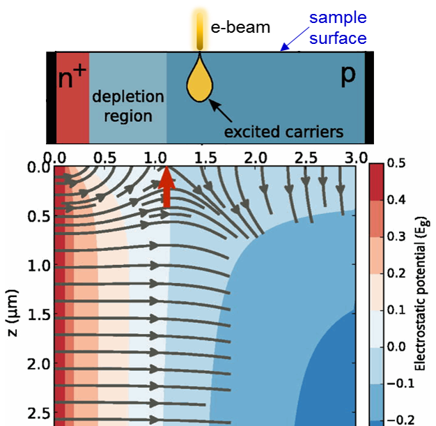
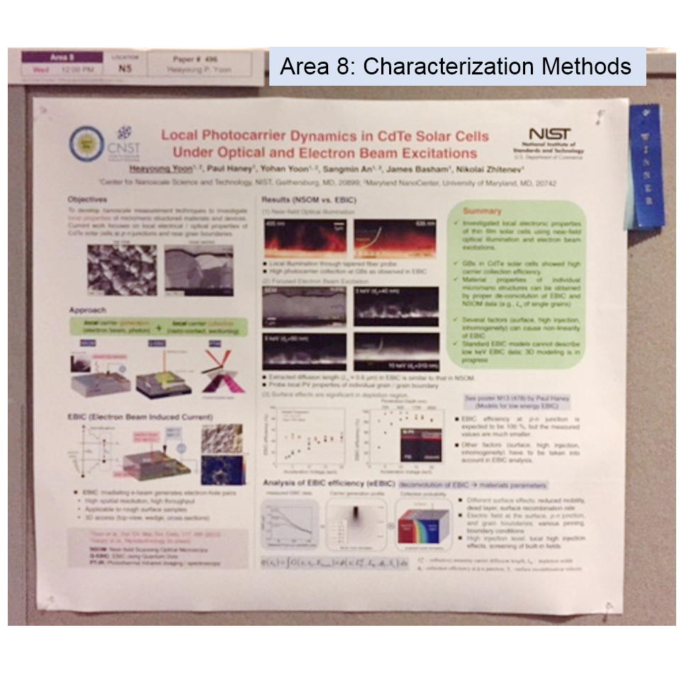
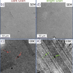
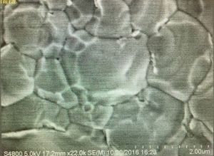
ABSTRACT:  We fabricate thin epitaxial crystal silicon solar cells on display glass and fused silica substrates overcoated with a silicon seed layer. To confirm the quality of hot-wire chemical vapor deposition epitaxy, we grow a 2-μm-thick absorber on a (100) monocrystalline Si layer transfer seed on display glass and achieve 6.5% efficiency with an open circuit voltage (V_OC) of 586mV without light-trapping features. This device enables the evaluation of seed layers on display glass. Using polycrystalline seeds formed from amorphous silicon by laser-induced mixed phase solidification (MPS) and electron beam crystallization, we demonstrate 2.9%, 476mV (MPS) and 4.1%, 551mV (electron beam crystallization) solar cells. Grain boundaries likely limit the solar cell grown on the MPS seed layer, and we establish an upper bound for the grain boundary recombination velocity (S_GB) of 1.6×104 cm/s.

LINK